

Multi-layer flash-memory device, a solid hard disk and a truncation non-volatile memory system
A non-volatile, memory technology, used in static memory, read-only memory, information storage, etc., can solve the problem of short service life of flash memory devices, and achieve the effect of prolonging the service life
- Summary
- Abstract
- Description
- Claims
- Application Information
AI Technical Summary
Problems solved by technology
Method used
Image

Examples
Embodiment Construction
[0076] In order to make the object, technical solution and advantages of the present invention clearer, the present invention will be further described in detail below in conjunction with the accompanying drawings and embodiments. It should be understood that the specific embodiments described here are only used to explain the present invention, not to limit the present invention.
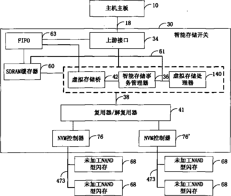
[0077] Figure 1A Demonstrated a smart memory switch interfaced with raw NAND-type flash memory devices. The smart storage switch 30 is connected to the host storage bus 18 through an upstream interface 34 . The smart storage switch 30 is also connected to the unprocessed NAND flash memory chip 68 through a physical block address (PBA) bus 473 . After the transactions from the virtual storage bridge 42 on the logical block address bus (logical block address, LBA) 38 are demultiplexed by the multiplexer / demultiplexer 41, they are sent to an NVM controller 76, and the NVM controller 76 converts the ...
PUM
 Abstract
Description
Claims
Application Information