
Manufacturing method of circuit module

A circuit module and process technology, applied in circuits, semiconductor/solid-state device manufacturing, electrical components, etc., can solve the problems of rising circuit module manufacturing costs, large amount of resin, and difficulty in thinning circuit modules, so as to reduce manufacturing costs. Effect

Inactive Publication Date: 2010-06-09
MITSUMI ELECTRIC CO LTD
View PDF5 Cites 2 Cited by
  • Summary
  • Abstract
  • Description
  • Claims
  • Application Information

AI Technical Summary

Problems solved by technology

[0021] However, circuit modules with existing COB configurations such as image 3 as well as Figure 4 As shown, since the electronic components are sealed with a sealing resin, the amount of resin used for sealing is large, and there is a problem that the manufacturing cost of the circuit module increases.
[0022] In addition, there are cases where the electronic components are thicker than the FET bare chip and the IC bare chip. In this case, since the FET bare chip and the IC bare chip including the electronic components are sealed with a sealing resin, it may be difficult to realize a circuit module. The problem of further thinning

Method used


Image

  • Manufacturing method of circuit module
  • Manufacturing method of circuit module
  • Manufacturing method of circuit module

Examples


no. 1 approach

[0051] Configuration of the circuit module related to the first embodiment of the present invention

[0052] First, the structure of the circuit module according to the first embodiment of the present invention will be described. Figure 7 It is a plan view illustrating the circuit module according to the first embodiment of the present invention. Figure 8 is along Figure 7 Sectional view of line C-C. refer to Figure 7 as well as Figure 8 , the circuit module 10 has a substrate 11a, wiring patterns 12a and 12b, through holes 13, solder protection layers 14a and 14b, adhesive 15, FET bare chip 16, bonding wire 16a, IC bare chip 17, bonding wire 17a, paste Solder material 18 , electronic component 19 , and sealing resin 20 .

[0053] In the circuit module 10, a wiring pattern 12a is formed on one surface of the substrate 11a, and a portion (hereinafter referred to as "pad") having an opening is formed on the wiring pattern 12a to be electrically connected to a mounted c...

Embodiment approach

[0077] According to the first embodiment of the present invention, by sealing only bare chips such as FETs and ICs with a sealing resin, compared with conventional circuit modules in which not only bare chips such as FETs and ICs are sealed but also electronic components, the cost can be reduced. The use amount of the materials constituting the sealing resin can suppress the increase of the manufacturing cost. In addition, by sealing only bare chips such as FETs and ICs with a sealing resin, even when electronic components are thicker than bare chips such as FETs and ICs, the overall thickness of the circuit module can be reduced (low profile) . Furthermore, since the area of ​​the sealing resin in the portion in contact with the substrate is smaller than that of a conventional circuit module, warping of the substrate can be reduced.

[0078] Furthermore, according to the first embodiment of the present invention, since the circuit module is manufactured in the order of the b...

no. 2 approach

[0082] Configuration of the circuit module related to the second embodiment of the present invention

[0083] First, the structure of the circuit module according to the second embodiment of the present invention will be described. Figure 17 It is a plan view illustrating the circuit module according to the second embodiment of the present invention. Figure 18 is along Figure 17 Sectional view of E-E line. exist Figure 17 as well as Figure 18 In, about with Figure 7 as well as Figure 8 The same symbols are attached to the same parts, and descriptions thereof may be omitted. refer to Figure 17 as well as Figure 18 , the circuit module 30 will Figure 7 as well as Figure 8 The FET bare chip 16 and IC bare chip 17 of the illustrated circuit module 10 are replaced with FET36 and IC37 of the CSP package, and the bonding wires 16a and 17a are replaced with terminals 36a and 37a. Other parts of the circuit module 30 are configured in the same manner as the circui...


PUM

PropertyMeasurementUnit
Thicknessaaaaaaaaaa
Thicknessaaaaaaaaaa

Abstract

The aim of the invention is to provide a manufacturing method which suppresses the increase of manufacturing cost and can realize further thinning. According to the manufacturing method of a circuit module according to the invention, the circuit module carries a semiconductor device on a substrate which is provided with a wiring pattern in a preset area, and furthermore the semiconductor component is sealed by sealing agent. The manufacturing method of the circuit is characterized by comprising the following steps: a first step of equipping the semiconductor component on the substrate; a second step of electrically connecting the semiconductor component with the wiring patter; a third step of sealing the semiconductor component with the sealing agent; and a fourth step of equipping electronic components on the area which is on the substrate and is not sealed by the sealing agent.

Description

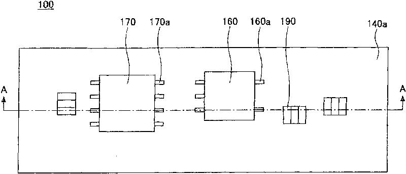
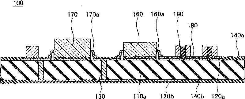
technical field [0001] The present invention relates to a method of manufacturing a circuit module in which semiconductor components are sealed with a sealant. Background technique [0002] Conventionally, a so-called COB (chip on board) structure has been used for circuit modules requiring miniaturization, such as a battery protection circuit module used as a power source of a portable device to protect a battery. The COB structure is a structure in which bare chips such as ICs and FETs are directly mounted on a substrate, electrically connected to wiring patterns on the substrate by wire bonding, etc., and then sealed with resin. By adopting the COB structure, it is possible to reduce the thickness of the circuit module compared with the discrete structure. Specific examples are shown below. [0003] figure 1 It is a plan view illustrating a conventional discrete structure circuit module. figure 2 is along figure 1 Sectional view of line A-A. refer to figure 1 as w...

Claims


Application Information

Patent Timeline
IPC IPC(8): H01L21/50H01L21/60H01L21/56H01L21/58
CPCH01L2224/48225H01L25/0655H01L2924/19105H01L2224/45144H01L24/48H01L2224/16225H01L2224/73265H01L23/3114H01L2224/48227H01L2224/32225H01L24/73H01L2924/181H01L2224/48H01L2924/00H01L2924/00012H01L23/28
Inventor 明石贵和高山裕树
Owner MITSUMI ELECTRIC CO LTD
Learn More