Back-illuminated mercury cadmium telluride long-wave light-guide type infrared flat-panel detector

A mercury cadmium telluride and detector technology, which is applied in the field of photoelectric detectors, can solve the problems of small gaps between photosensitive surfaces of arrays and the inability to arrange signal leads, and achieve the effects of easy wiring, solving heat conduction problems, and ensuring imaging quality

Active Publication Date: 2010-06-09
SHANGHAI INST OF TECHNICAL PHYSICS - CHINESE ACAD OF SCI
View PDF0 Cites 15 Cited by
  • Summary
  • Abstract
  • Description
  • Claims
  • Application Information

AI Technical Summary

Problems solved by technology

[0003] The purpose of the present invention is to provide a back-illuminated detector structure suitable for mercury cadmium telluride long-wave photoconductive infrared area detectors, and to solve the current requirement that the gap between the photosensitive surfaces of the array is small through the device of the back-illuminated structure. As a result, the problem that the signal leads cannot be arranged

Method used


Image

  • Back-illuminated mercury cadmium telluride long-wave light-guide type infrared flat-panel detector
  • Back-illuminated mercury cadmium telluride long-wave light-guide type infrared flat-panel detector

Examples


Embodiment Construction

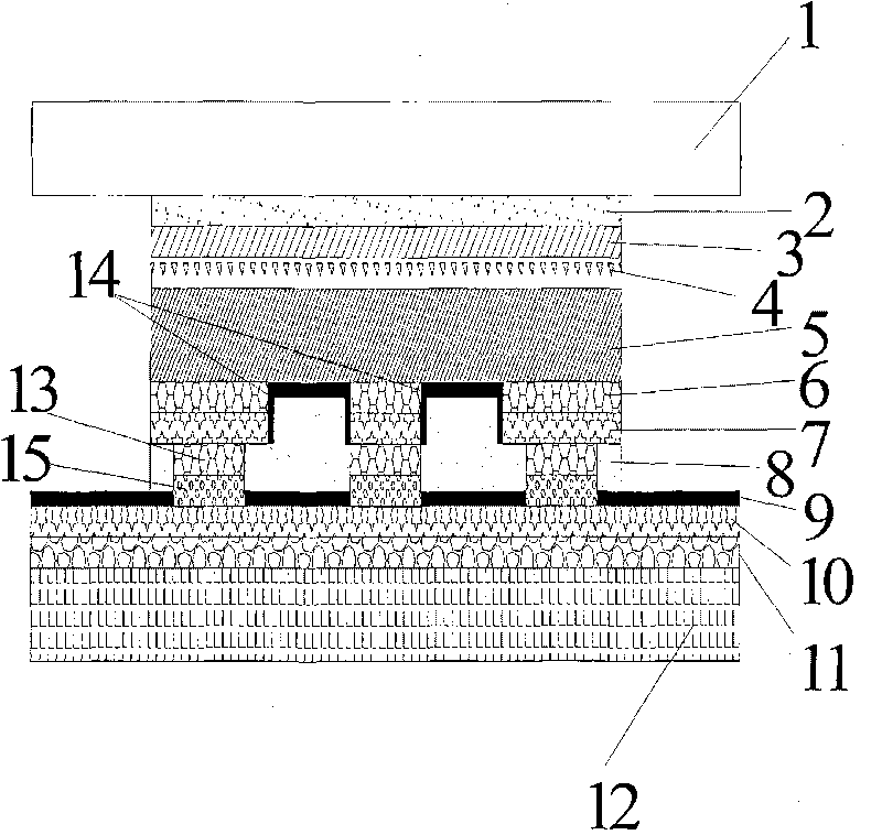
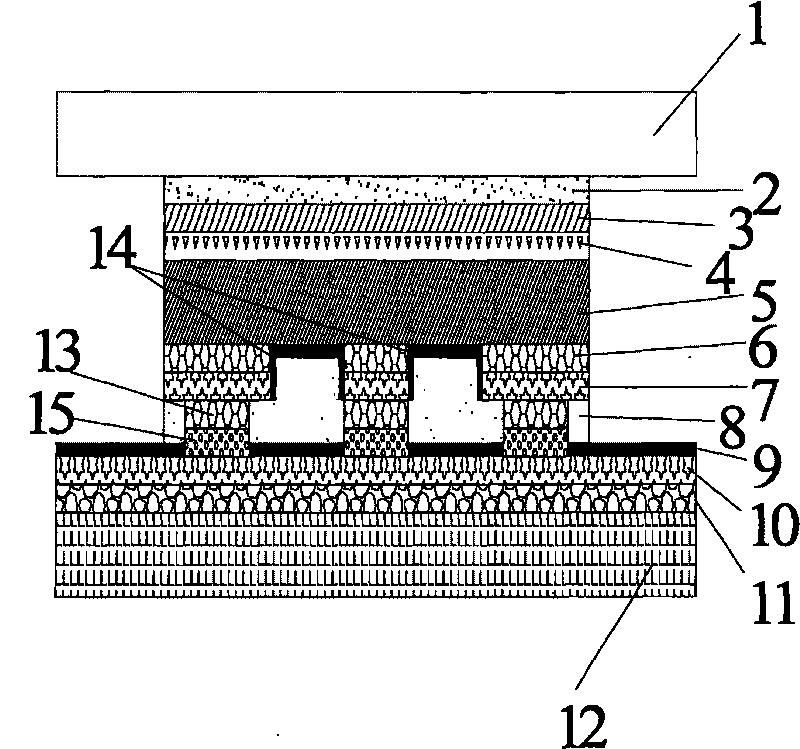
[0015] Combined with the accompanying drawings of the specification, taking the 8×8 back-illuminated HgCdTe long-wave photoconductive infrared area detector as an example, this patent will be further described in detail. The process used is the conventional process for forming HgCdTe chips:

[0016] 1. The first surface treatment: the first surface of the selected mercury cadmium telluride material is subjected to a series of treatments such as rough grinding to remove 100 μm, polishing to remove 40 μm, and chemical etching to remove 3 μm. After removing the damage, a layer is grown The anodized layer (4) is used as a passivation film, and another layer is grown on the entire surface anti-reflection layer (3);

[0017] 2. SMT: Use low-temperature epoxy glue (2) to paste the HgCdTe material on the first side and the zinc selenide substrate (1) together, and cure the epoxy glue in a fully automatic tablet press , since what we are preparing is a long-wave device, we should tr...


PUM


Abstract

The invention discloses a back-illuminated mercury cadmium telluride long-wave light-guide type infrared flat-panel detector. The detector is characterized by comprising a zinc selenide substrate and a mercury cadmium telluride sheet fixed on the substrate by epoxy glue, wherein one face of the mercury cadmium telluride sheet, which is in contact with the substrate, is provided with an anodized layer and a ZnS anti-reflection layer, and the double-layer passivation surface on the surface of the mercury cadmium telluride sheet forms an a photosensitive element area array and a signal extraction electrode area and a common electrode area which are respectively positioned at both ends of a photosensitive element by photoengraving. The signal extraction electrode area and the common electrode area are both extracted from the back side of a light collection surface, an indium bump grows in a specified area, another indium bump grows on a signal reading circuit board, and the indium bumps are interconnected. An indium bump of a chip electrode and an indium bump of an electrode plate are connected together. An indium layer, an aurum layer and indium bumps are orderly grow on the signal electrode area and the common electrode area, thereby forming the back-illuminated mercury cadmium telluride long-wave light-guide type infrared flat-panel detector.

Description

technical field [0001] The invention relates to photoelectric detector technology, in particular to a back-illuminated mercury cadmium telluride long-wave photoconductive infrared area detector. Background technique [0002] With the development of the application field of infrared devices, the resolution requirements for devices are getting higher and higher, from unit to line array, and now to area array. For use, the area array detector requires the larger the duty cycle, the better, that is to say, within a given area of ​​the area array device, the larger the proportion of the photosensitive surface, the better, and the smaller the interval between the photosensitive surfaces, the better. Since each photosensitive element of the area array has a lead arrangement, it is hoped that the distance between the photosensitive surfaces should be as large as possible. At present, our mercury cadmium telluride long-wave photoconductive infrared area array device adopts the tradit...

Claims


Application Information

Patent Timeline
Patent Type & Authority Applications(China)
IPC IPC(8): H01L27/144H01L23/498H01L21/60G01J1/02
CPCH01L2224/73204
Inventor 赵水平朱龙源李向阳刘诗嘉兰添翼王妮丽蔡子健贾嘉
Owner SHANGHAI INST OF TECHNICAL PHYSICS - CHINESE ACAD OF SCI
Why Eureka
Try Eureka