Multi-wavelength light-emitting diode and production method thereof

A light-emitting diode and multi-wavelength technology, which is applied in the direction of electrical components, circuits, semiconductor devices, etc., can solve the problems of easily changing p-n junctions, damaging the luminescent characteristics or electrical characteristics of components, and poor conversion efficiency of red phosphor powder, so as to reduce pollution Opportunity, effect of increasing light extraction efficiency

Inactive Publication Date: 2010-06-09
ZHANJING TECH SHENZHEN +1
View PDF13 Cites 18 Cited by
  • Summary
  • Abstract
  • Description
  • Claims
  • Application Information

AI Technical Summary

Problems solved by technology

[0007] All the prior art listed above place the luminescent material of the second wavelength between the n-type conductive layer and the p-type conductive layer. This technology is easy to change the distribution of the p-n junction (junction), thereby damaging the luminescent characteristics of the element or electrical characteristics
However, some previous proposals still need to add phosphors during packaging, but the current conversion efficiency of this red phosphor is still poor.
Furthermore, some previous proposals required adding a photolithography process to the two epitaxial processes, which was cumbersome and had doubts about the process yield.

Method used


Image

  • Multi-wavelength light-emitting diode and production method thereof
  • Multi-wavelength light-emitting diode and production method thereof
  • Multi-wavelength light-emitting diode and production method thereof

Examples


Embodiment Construction

[0041]The direction of the present invention discussed here is a light emitting diode and its technology. In order to provide a thorough understanding of the present invention, detailed steps and components thereof will be set forth in the following description. Obviously, the practice of the invention is not limited to the specific details familiar to those skilled in light emitting diodes and their art. On the other hand, well-known components or steps have not been described in detail so as not to unnecessarily limit the invention. Preferred embodiments of the present invention will be described in detail as follows, however, in addition to these detailed descriptions, the present invention can also be widely implemented in other embodiments, and the scope of the present invention is not limited, it is based on the appended claims .

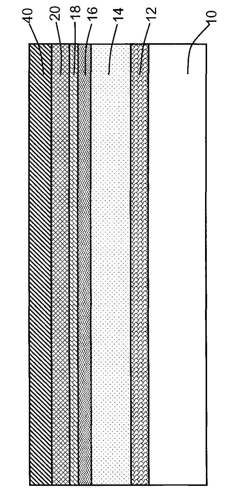
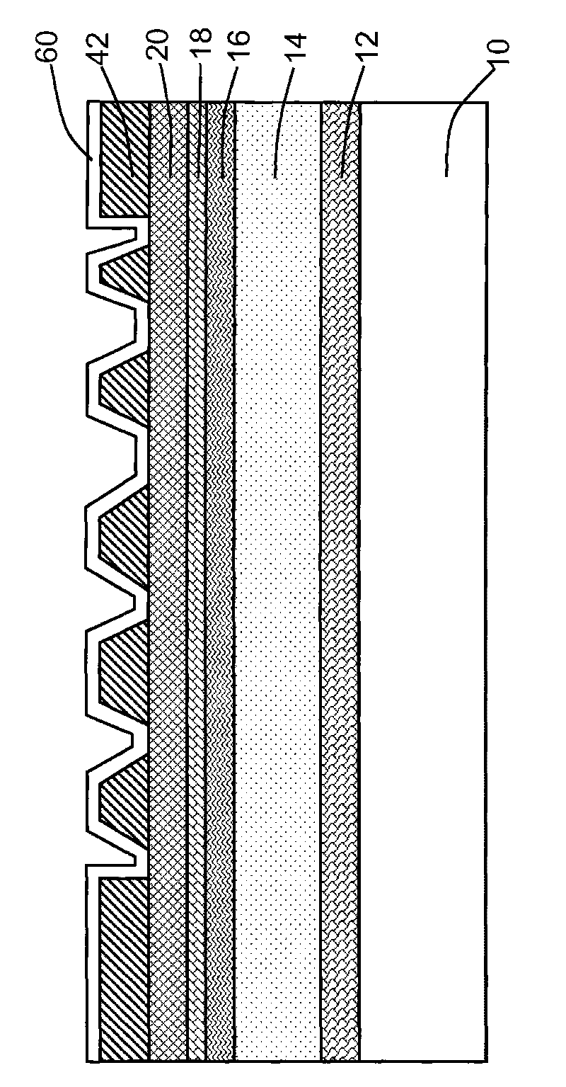
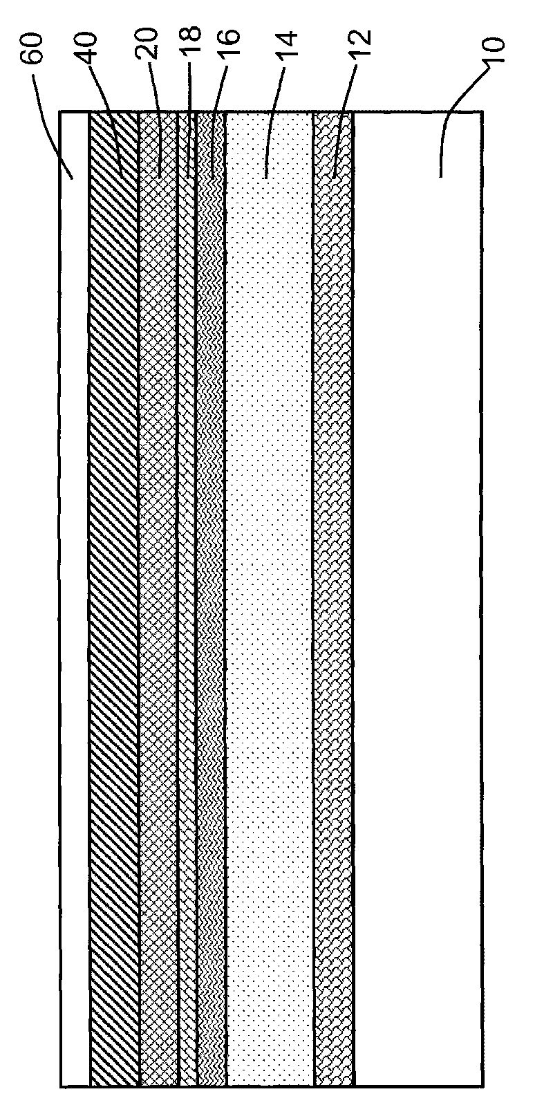
[0042] The present invention utilizes the process of growing at least one wavelength conversion material on the surface of the light-emitti...


PUM


Abstract

The invention adopts the processes of growing at least a wavelength conversion material on the surface of a light-emitting component, converting part of light from the light-emitting component into at least one light with different wavelength and mixing the light with different wavelength with the light which comes from the light-emitting component but is not converted to finally obtain the required light source of a CIE coordinate. The whole process of the wavelength conversion material layer formed in the invention can be completed in an epitaxial reactor, without additional yellow photolithography process, thus reducing the probability of pollution of epitaxial wafers. In addition, compared with many light-emitting components in the prior art, the light-emitting component in the invention is characterized in that the p-n junction position can not be changed and the light-emitting efficiency can be retained. Furthermore, the wavelength conversion material is a compound semiconductor and the required wavelength can be randomly changed according to the energy level of the material. Meanwhile, coarsened surface can be formed on the wavelength conversion material layer, thus increasing the light extraction efficiency of the component.

Description

technical field [0001] The invention relates to a light-emitting diode and a manufacturing method thereof, in particular to a multi-wavelength light-emitting diode and a manufacturing method thereof. Background technique [0002] In the current light-emitting diode technology, commercialized white light-emitting diodes use three primary colors of red, green and blue to mix colors into white light. However, this method has a disadvantage in that the light mixing of the three-color light-emitting diodes is not easy. When applied to the backlight of liquid crystal display, technologies such as diffusion plate and brightness enhancement film can also be used to allow uniform color mixing of various colors of light. However, when applied in lighting, it is not easy to provide a uniformly mixed white light. At the same time, since the lifetimes of the three light emitting diodes are generally different, if one of the color light emitting diodes fails or is damaged, the color inc...

Claims


Application Information

Patent Timeline
Patent Type & Authority Applications(China)
IPC IPC(8): H01L33/00
Inventor 黄世晟涂博闵叶颖超林文禹吴芃逸詹世雄
Owner ZHANJING TECH SHENZHEN
Why Eureka
Try Eureka