High gain amplifier circuit

An amplifier circuit, high-gain technology, applied to amplifiers with only semiconductor devices, amplifiers with at least 3 electrodes or two PN junctions, etc., can solve the problem of consuming chip area and power consumption, increasing chip area and power consumption , input swing range limitation, etc., to achieve the effect of large input swing, high intrinsic gain, and wide input swing range

Active Publication Date: 2010-06-09
SOUTH CHINA UNIV OF TECH
View PDF0 Cites 13 Cited by
  • Summary
  • Abstract
  • Description
  • Claims
  • Application Information

AI Technical Summary

Problems solved by technology

In the cascode structure, the gates of each cascaded transistor are connected to different bias voltages, the number of bias voltages is large, the bias circuit is complicated, and a large amount of chip area and power consumption are consumed; due to the cascode structure The bias voltage cannot follow the change of the input signal, the input swing range is limited, and the swing range is small
The multi-level cascaded structure doubles the chip area and power consumption, and the cost is high. It also increases the number of poles in the circuit, making the stability of the circuit a prominent problem, which in turn requires a complex frequency compensation circuit to stabilize the amplifier.
The gain enhancement technology is based on the cascode structure, which makes the bias circuit more complicated

Method used


Image

  • High gain amplifier circuit
  • High gain amplifier circuit
  • High gain amplifier circuit

Examples


Embodiment 1

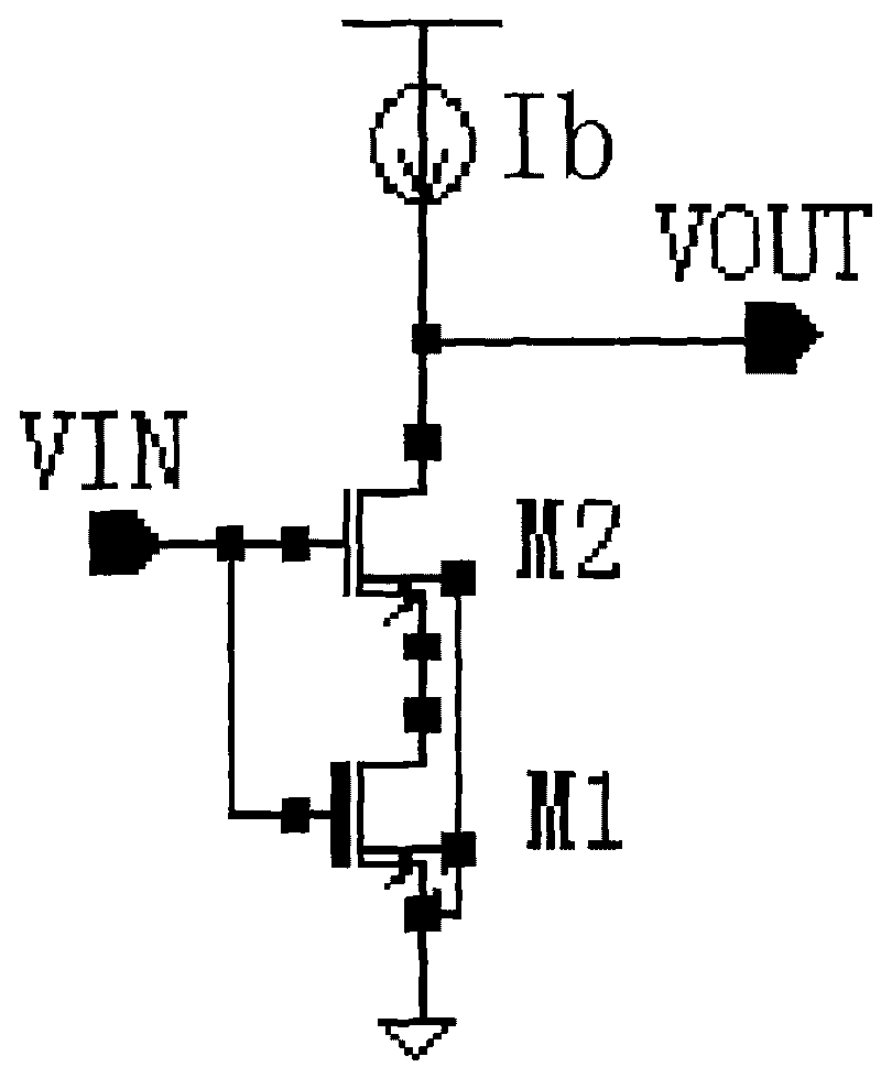
[0032] figure 1 Two transistors, transistors M1 and M2, are used in the circuit; more than two transistors can be cascaded according to actual needs.

[0033] figure 1 , the current source Ib should be a current source with a large output resistance, which can be a cascode transistor structure or a cascode structure similar to the gates of M1 and M2 connected. The current flowing from the current source Ib is collected by the drain of the transistor M2, and the drain of M2 is the output node VOUT. The DC voltage signal of the input signal VIN provides a static gate bias voltage for the cascaded transistors M1 and M2. The gate oxide layer of transistor M1 is thicker than that of transistor M2, and the turn-on voltage V of transistor M1 T1 than the turn-on voltage of transistor M2 V T2 High, and the gate-source voltage Vgs2 of transistor M2 is not greater than the turn-on voltage V of transistor M1 T1 , Transistors M1 and M2 are both working in the amplified state.

[0034...

Embodiment 2

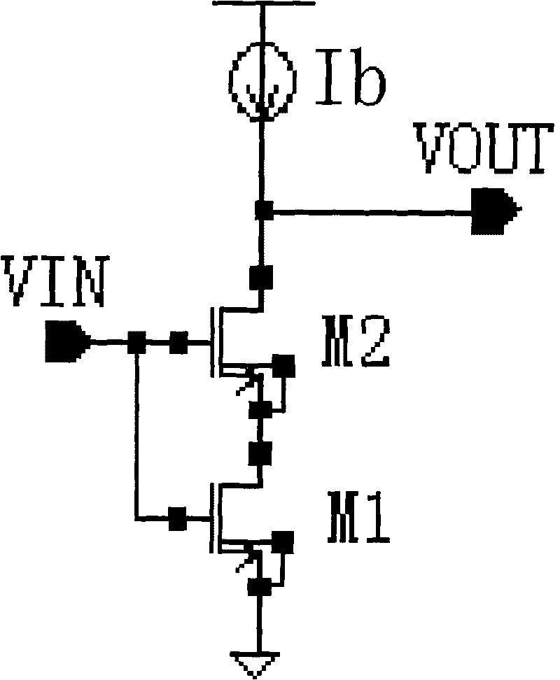
[0038] figure 2 , the current source Ib should be a current source with a large output resistance, which can be a cascode transistor structure or a cascode structure similar to the gates of M1 and M2 connected. The current flowing from the current source Ib is collected by the drain of the transistor M2, and the drain of M2 is the output node VOUT. The DC voltage signal of the input signal VIN provides a static gate bias voltage for the cascaded transistors M1 and M2. The turn-on voltages of the transistors M1 and M2 are equal, and both the transistors M1 and M2 work in an amplified state. The transistor M1 works in a saturated state, the transistor M2 works in a subthreshold state, and the gate-source voltage Vgs2 of M2 is not greater than the turn-on voltage of M1.

[0039] The intrinsic gain (VOUT node to VIN node) of cascaded transistors M1, M2 is

[0040] Av=g m1 g m2 r o1 r o2

[0041] Among them, g mi is the transconductance of transistor Mi, r oi is the drai...

Embodiment 3

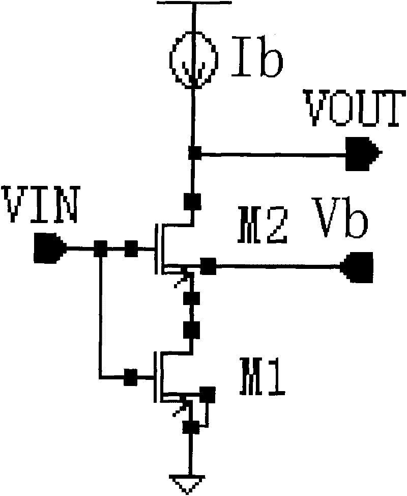
[0043] image 3 , the current source Ib should be a current source with a large output resistance, which can be a cascode transistor structure or a cascode structure similar to the gates of M1 and M2 connected. The current flowing from the current source Ib is collected by the drain of the transistor M2, and the drain of M2 is the output node VOUT. The DC voltage signal of the input signal VIN provides a static gate bias voltage for the cascaded transistors M1 and M2. The substrate of the transistor M2 is connected to the bias voltage Vb, so that the turn-on voltage of the transistor M2 is lower than the turn-on voltage of the transistor M1. If the forward conduction voltage of the PN junction is smaller than the gate-source voltage Vgs2 of the transistor M2, the bias voltage Vb can be VIN. If the drain-source voltage of the transistor M2 is lower than the forward conduction voltage of the PN junction, the bias voltage Vb can be VOUT. The bias voltage Vb can be a dynamic or...


PUM


Abstract

The invention relates to a high gain amplifier circuit which is formed by a cascade transistors structure. The grids of the cascade transistors are connected together and the source drains are orderly connected serially. Each cascade transistor is in an amplifying state and has high output impedance and high gain. The amplifier circuit is characterized by high gain, wide input swing range and simple grid polarization. The invention is fit for the application places requiring high gain, big swing and low power consumption.

Description

technical field [0001] The design of the present invention relates to analog integrated circuits, especially high-gain amplifier circuits. Background technique [0002] The amplifier acts as the basic unit circuit in the integrated circuit, and its performance directly affects the performance of the circuit system. The design of the amplifier is often the key to the design of an analog integrated circuit. A typical high-gain amplifier circuit adopts cascode structure, multi-stage cascaded structure, and gain enhancement technology. In the cascode structure, the gates of each cascaded transistor are connected to different bias voltages, the number of bias voltages is large, the bias circuit is complicated, and a large amount of chip area and power consumption are consumed; due to the cascode structure The bias voltage cannot follow the change of the input signal, the input swing range is limited, and the swing range is small. The multi-level cascaded structure doubles the c...

Claims


Application Information

Patent Timeline
Patent Type & Authority Applications(China)
IPC IPC(8): H03F3/14
Inventor 姚若河卞振鹏
Owner SOUTH CHINA UNIV OF TECH
Why Eureka
Try Eureka