Supercharge Your Innovation With Domain-Expert AI Agents!

Esd protection circuit and circuitry of ic applying the ESD protection circuit

An electrostatic discharge protection, electrostatic discharge technology, applied in emergency protection circuit devices, emergency protection circuit devices for limiting overcurrent/overvoltage, circuits, etc., can solve the problems of increasing chip size and VLSI circuit size. , to avoid damage

Active Publication Date: 2010-06-16
MEDIATEK INC
View PDF0 Cites 8 Cited by
  • Summary
  • Abstract
  • Description
  • Claims
  • Application Information

AI Technical Summary

Problems solved by technology

If the wire width of the VLSI circuit is increased, the VLSI circuit can tolerate or tolerate a larger ESD current, but the size of the VLSI circuit will increase
In addition, increasing the circuitry within the chip also increases the size of the chip

Method used


Image

  • Esd protection circuit and circuitry of ic applying the ESD protection circuit
  • Esd protection circuit and circuitry of ic applying the ESD protection circuit
  • Esd protection circuit and circuitry of ic applying the ESD protection circuit

Examples


Embodiment Construction

[0017] The following description is of the preferred contemplated mode of carrying out the invention. This description serves only to illustrate the principles of the present invention, and not to limit the present invention. The protection scope of the present invention should be defined by the scope of the appended claims.

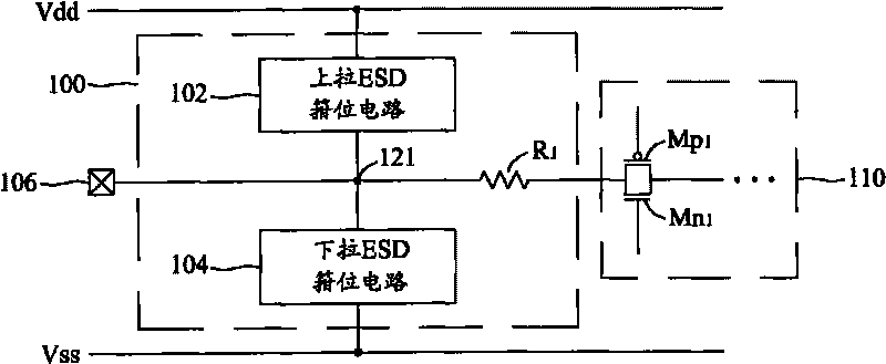
[0018] figure 1 is a schematic diagram of an integrated circuit including an ESD protection circuit 100 . The ESD protection circuit 100 blocks ESD from the input / output pad unit (I / O pad, hereinafter referred to as I / O pad unit) 106 to the internal circuit 110 . The ESD protection circuit 100 includes a pull up (PU) ESD clamp circuit 102 , a pull down (PD) ESD clamp circuit 104 and a resistor R1 . The I / O pad unit 106 is coupled to the node 121 for receiving or transmitting signals. The pull-up ESD clamping circuit 102 is coupled between the first voltage path (ie, the voltage path whose voltage level is Vdd) and the node 121, and is used for clampi...


PUM


Abstract

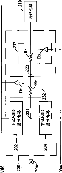
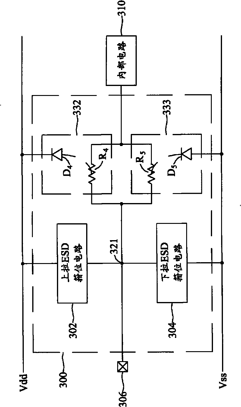
A circuitry of an IC is provided, including a pad, an internal circuit, and an ESD protection circuit. The pad transmits or receives a signal and is coupled to a first node. The internal circuit is coupled to the first node for processing the signal. The ESD protection circuit includes an ESD clamping circuit, a first current limiting and shunting unit and a second current limiting and shunting unit. The ESD clamping circuit is coupled to the first node, for clamping an ESD current flowing through the first node. The first current limiting and shunting unit is through the first node coupled to the pad, for limiting the ESD current and shunting part of the ESD current to a first voltage path. The second current limiting and shunting unit is coupled to the first current limiting and shunting unit, for limiting the ESD current and shunting part of the ESD current to a second voltage path.

Description

technical field [0001] The present invention relates to an electrostatic discharge (ESD) protection circuit and an integrated circuit, and more particularly, to an ESD protection circuit and an integrated circuit using a diffusion resistor and a parasitic diode. . Background technique [0002] From the perspective of the development of semiconductor manufacturing process, the size of complementary metal-oxide-semiconductor (hereinafter referred to as CMOS) transistors has reached the sub-micron level, which improves the very large scale integration. , hereinafter referred to as VLSI) circuit performance and calculation speed. As the size of the VLSI circuit is reduced, the ESD tolerance and reliability of the VLSI circuit are also greatly reduced. [0003] The ESD model includes a human-body model (HBM), a machine model (MM) and a charged-device model (CDM). All three models generate transient currents of several amperes that last only for hundreds or even nanoseconds. ...

Claims


Application Information

Patent Timeline
Patent Type & Authority Applications(China)
IPC IPC(8): H02H9/02H01L23/60
CPCH01L27/0251H01L27/0288
Inventor 林奕成
Owner MEDIATEK INC
Features
  • R&D
  • Intellectual Property
  • Life Sciences
  • Materials
  • Tech Scout
  • Unparalleled Data Quality
  • Higher Quality Content
  • 60% Fewer Hallucinations
Learn More