

Modulation method and implementation circuit for unit vector to carrying out time-delay superimposition of multi-level space vector
A modulation method and space vector technology, which are applied to electrical components, output power conversion devices, and AC power input to DC power output, etc., can solve problems such as complex calculation methods, achieve convenient and flexible control, improve control performance, reduce The effect of system resource requirements
- Summary
- Abstract
- Description
- Claims
- Application Information
AI Technical Summary
Problems solved by technology
Method used
Image

Examples
specific Embodiment approach 1
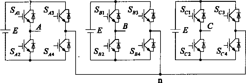
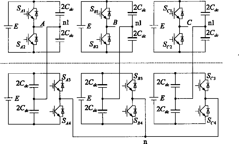
[0014] Specific implementation mode one: the following combination Figure 1-Figure 4 Describe this embodiment, this embodiment comprises the following steps:
[0015] Step 1: The left bridge arm and the right bridge arm of the three H-bridge inverters of each level unit of the three-phase N-level unit cascaded inverter are equivalent to the left bridge arm equivalent inverter and the right bridge arm respectively Arm equivalent inverter, so that the output voltage vector of each level unit of the three-phase N-level unit cascaded inverter is equivalent to the output voltage vector of the left bridge arm equivalent inverter and the right bridge arm equivalent inverter The difference, N is a natural number greater than 1;
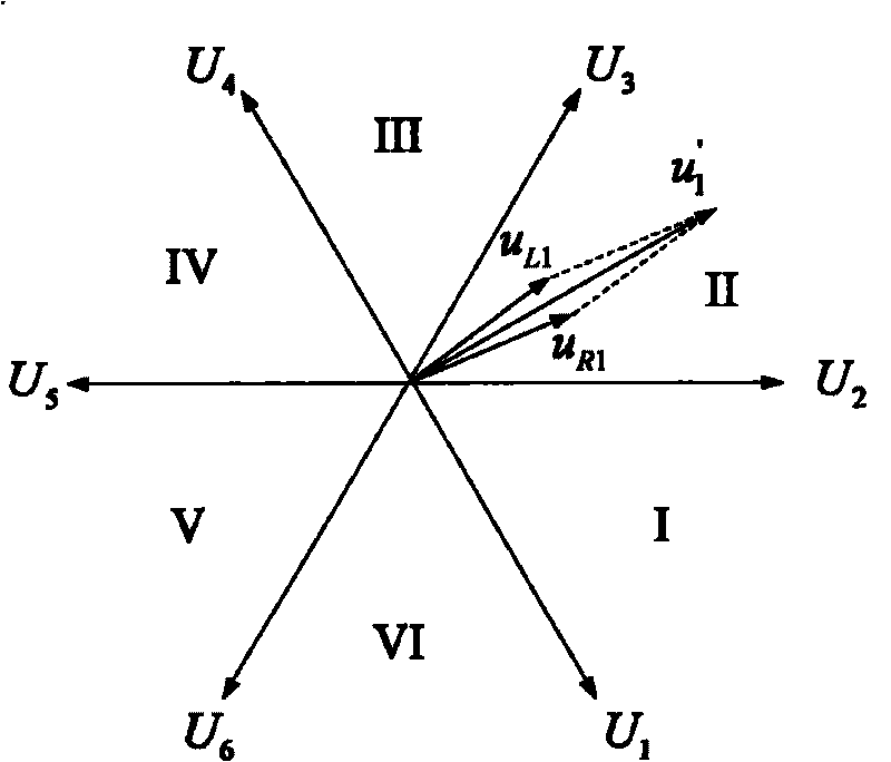
[0016] Step 2: Set the calculation period of the three-phase N-level unit cascaded inverter as T s , the number of units is i, i is a natural number and i≤N, at the beginning of each calculation cycle, the left side of the first-level unit of the three-pha...
specific Embodiment approach 2
[0028] Specific implementation mode two: the following combination Figure 5-Figure 8 Describe this embodiment, this embodiment is made up of DSP chip 1 and FPGA field programmable gate array 2, and FPGA field programmable gate array 2 is made up of data latch module 2-1, decoding module 2-2, voltage vector module 2- 3. Dead time module 2-4, PWM control module 2-5, counter period value module 2-6, counter group 2-7, N PWM generators 2-8 and N signal interlock modules 2-9 ,
[0029] The control data output end of DSP chip 1 is connected to the control data input end of data latch module 2-1, the address signal output end of DSP chip 1 is connected to the address signal input end of decoding module 2-2, and the address signal input end of decoding module 2-2 The module selection enable signal output terminal is connected to the address signal input terminal of the data latch module 2-1, wherein the address signal received by the data latch module 2-1 corresponds to the control ...
PUM
 Abstract
Description
Claims
Application Information