Avalanche energy tester of power MOSFET device

A tester and device technology, applied in the field of power MOSFET device avalanche energy tester, can solve problems such as the inability to provide high instantaneous current power MOSFET avalanche energy test, and achieve the effect of improving test ability

Inactive Publication Date: 2010-06-23
西安明泰半导体科技有限公司
View PDF0 Cites 19 Cited by
  • Summary
  • Abstract
  • Description
  • Claims
  • Application Information

AI Technical Summary

Problems solved by technology

[0005] The purpose of the present invention is to provide a power MOSFET device avalanche energy tester, which sol

Method used


Image

  • Avalanche energy tester of power MOSFET device
  • Avalanche energy tester of power MOSFET device
  • Avalanche energy tester of power MOSFET device

Examples


Embodiment Construction

[0021] The present invention will be described in detail below in conjunction with the accompanying drawings and specific embodiments.

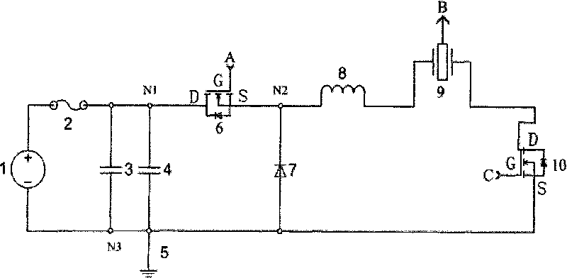
[0022] The power MOSFET device avalanche energy tester of the present invention comprises a front-end avalanche test circuit and a back-end avalanche current sampling circuit.

[0023] like figure 1 As shown, the hardware structure of the front-end avalanche test circuit is: including a 0-50V adjustable DC power supply 1, the positive pole of the adjustable DC power supply 1 is connected to the 1A fuse 2; the other end of the fuse 2 is connected to the MOSFET device 6 (selected model is The drain of IXFX140N30P) is connected; the source of MOSFET device 6 is connected with one end of inductor 8; the other end of inductor 8 is connected with the current input end of current inductor 9; the current output end of current inductor 9 is connected with MOSFET device 10 to be tested The drain of the MOSFET device 10 to be tested is connected to the...


PUM


Abstract

The invention discloses an avalanche energy tester of a power MOSFET device, comprising a front-end avalanche testing circuit and a back-end avalanche current sampling circuit. The hardware structure of the front-end avalanche testing circuit comprises an adjustable direct current power supply which is connected with a fuse, an MOSFET device, an inductor, a current sensor and an MOSFET device to be tested successively to form a circuit; an electrolytic capacitor and a ceramic capacitor are paralleled between the drain electrode of the MOSFEF device and the source electrode of the MOSFET device to be tested; a diode is connected between the source electrode of the MOSFET device and the source electrode of the MOSFET device to be tested; and the structure of the back-end avalanche current sampling circuit is as follows: a signal conditioning circuit and a reference source circuit are connected with an analog-to-digital converter, and the analog-to-digital converter is connected with an FPGA control logic which is respectively connected with a test machine signal connector, an MOS driving circuit and a separator signal connector. The tester in the invention can provide high instantaneous current to test the avalanche energy.

Description

technical field [0001] The invention belongs to the technical field of semiconductor testing, and relates to an avalanche energy tester for power MOSFET devices. Background technique [0002] Power MOSFET devices are widely used in power electronic equipment due to their advantages such as simple manufacturing process, high integration, strong anti-interference ability, fast speed, low power consumption, and low price. With the rapid development of semiconductor technology and the in-depth understanding of reliability and failure modes, chip design manufacturers have also brought new challenges. Therefore, how to make products safer, more reliable, and have a longer life under the condition of ever-shrinking chip size has become a huge challenge faced by all major power semiconductor manufacturers today. Especially for the wide application of power MOSFETs in special working environments such as high-frequency switching and automotive electronics, the failure of UIS (the ab...

Claims


Application Information

Patent Timeline
IPC IPC(8): G01R22/00G01R31/26
Inventor 李志强
Owner 西安明泰半导体科技有限公司
Why Eureka
Try Eureka