

Multijunction gallium arsenide solar cell
A solar cell, gallium arsenide technology, applied in the field of solar cells, can solve problems such as the reduction of solar cell efficiency, and achieve the effects of improving current density, reducing reflection, and improving conversion efficiency
- Summary
- Abstract
- Description
- Claims
- Application Information
AI Technical Summary
Problems solved by technology
Method used
Image

Examples
Embodiment Construction
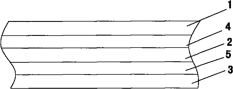
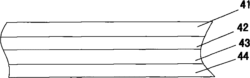
[0012] see figure 1 , figure 2 , the multi-junction gallium arsenide solar cell of the present invention includes a top cell 1 composed of AlInP (n+, 35nm) / GaInP (n / p, 520nm) / AlInP (p+, 120nm), and a top cell 1 composed of AlInP (n+, 120nm) / InGaAs(n / p, 3.5μm) / AlGaAs(p+, 100nm) composed of medium cell 2 and GaInP(n + , 100nm) / Ge(n + , 100nm) / Ge(p + , 170μm) constitutes the bottom cell 3, between the top cell and the middle cell is provided with AlInP (p + ) / AlGaAs(p ++ )-GaInP(n ++ ) / AlInP(n + ) or AlGaInP (p + ) / AlGaAs(p ++ )-GaInP(n ++ ) / AlInP(n + ) to form a tunnel junction connection structure 4 . Among them, 41 represents AlInP (p + ) or AlGaInP (p + ), which is the back field of the top cell, with a thickness of 100nm to 150nm; 44 represents AlInP(n + ), which is the back field of the battery, with a thickness of 100nm to 150nm; 42 means AlGaAs (p ++ ), the thickness is 10nm ~ 15nm; 43 means GaInP (n ++ ), with a thickness of 10nm to 15nm. (p + ) means...
PUM
| Property | Measurement | Unit |
|---|---|---|
| Thickness | aaaaa | aaaaa |
Abstract
Description
Claims
Application Information