

Illuminating device
A technology of light-emitting devices and light-emitting diodes, which is applied in the direction of electrical components, circuits, semiconductor devices, etc., can solve the problems of chromaticity accuracy or finished product pass rate of light-emitting device products, and the thickness of the wavelength conversion layer is not uniform enough, etc., to improve the chromaticity Accuracy or qualified rate of finished products, avoiding the effect of errors
- Summary
- Abstract
- Description
- Claims
- Application Information
AI Technical Summary
Problems solved by technology
Method used
Image

Examples
no. 1 example
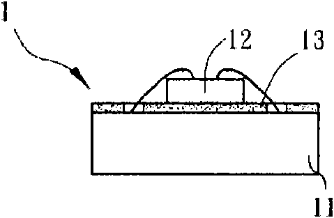
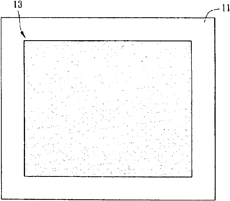
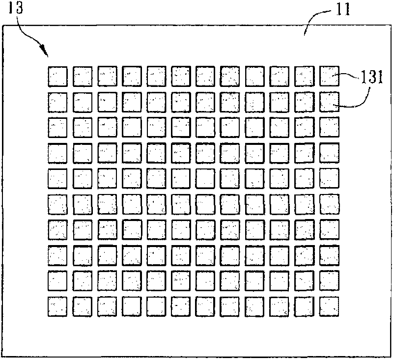
[0036] Please refer to figure 1 , which is a schematic diagram of the light emitting device 1 according to the first embodiment of the present invention. Wherein, the light emitting device 1 may be a lighting device, a backlight module of a liquid crystal display device, a billboard, or a light source module of other electronic devices. The lighting devices can be divided into indoor lighting devices or outdoor lighting devices. The indoor lighting devices are such as table lamps, fluorescent lamps or ceiling lamps, and the outdoor lighting devices are such as street lamps, indicator lights or traffic signals. The light emitting device 1 includes a substrate 11 , a light emitting diode 12 and a polished wavelength conversion layer 13 .
[0037] The substrate 11 can be, for example, a circuit substrate, and it can be a transparent substrate, and the material includes glass, or sapphire, or quartz, or plastic, or metal, or polymer material.
[0038] The light emitting diode 12...
no. 2 example
[0055] Please refer to Figure 6A and Figure 6B As shown, it is a schematic diagram of the light emitting device 2, 2a according to the second embodiment of the present invention. The difference between the light emitting device 2, 2a and the first embodiment is that: the light emitting device 2, 2a further includes a first carrier 24, the wavelength conversion layer 23 is arranged on the first carrier 24, and the wavelength conversion layer 23 and the first carrier 24 together set on the substrate 21 . exist Figure 6A In the illustration, the first carrier 24 is located between the substrate 21 and the wavelength conversion layer 23 for illustration, and the light emitting diode 22 is arranged on the wavelength conversion layer 23; and Figure 6B Then, the wavelength conversion layer 23 is located between the substrate 21 and the first carrier 24 for illustration. Wherein, each light emitting diode 22 is respectively arranged on the first carrier 24 , of course, a plura...
no. 3 example
[0062] Please refer to Figure 8 As shown, it is a schematic diagram of the light emitting device 3 according to the third embodiment of the present invention. The difference between the light emitting device 3 and the first embodiment is that the light emitting device 3 further includes a reflective layer 35 or a scattering layer, which is disposed on the same side or opposite sides of the substrate 31 as the wavelength converting layer 33 . In this embodiment, the reflective layer 35 and the wavelength conversion layer 33 are respectively disposed on opposite sides of the substrate 31 for illustration, but this is not limiting. In addition, the LED 32 is electrically connected to the bonding pad (not shown in the figure) on the substrate 31 in a flip-chip manner.
[0063] Therefore, at least a part of the light emitted by the LED 32 irradiates the wavelength conversion layer 33 and passes through the substrate 31 , is reflected or scattered by the reflective layer 35 or the...
PUM
 Abstract
Description
Claims
Application Information