
Multi-interface memory verification system based on FPGA

A verification system and memory technology, which is applied in the field of multi-interface memory verification systems based on field programmable gate arrays, can solve problems such as waste of resources, inability to test performance completely, and inability to completely simulate the actual use environment of high-speed memory, so as to shorten the effect of time period

Inactive Publication Date: 2010-07-07
EAST CHINA NORMAL UNIV
View PDF0 Cites 24 Cited by
  • Summary
  • Abstract
  • Description
  • Claims
  • Application Information

AI Technical Summary

Problems solved by technology

[0002] With the introduction of large-capacity and high-speed memories on the market, the increase in capacity and speed has led to differences in the details of the memory and the standard interface. The introduction of new types of memory has fundamentally changed the access interface of the memory and the operation of accessing it. However, mainstream controllers in the market cannot fully support direct access to such large-capacity, high-speed memories with special access interfaces.
[0003] At present, the mainstream test method of memory at home and abroad is still to test the chips of a single model or a single interface separately. There is no universal test platform for chips of different interface types (such as NOR Flash and SPI Flash), which leads to For memory chips with different functions, it is necessary to provide different test platforms for testing their functional integrity and performance stability, resulting in waste of resources
[0004] In addition, the domestic research also mostly stays on how to control the traditional single type of memory, which is not good for the process of putting the memory of various new interfaces into practical application. On the other hand, in the development based on FPGA, people are more accustomed to Use the imitation CPU soft and hard core resources embedded in the FPGA chip to complete many control tasks on the CPU side. Due to the limitation of the internal clock, these resources cannot completely simulate the possible actual use environment of the high-speed memory, and cannot fully test that it works at high speed. performance under the clock

Method used


Image

  • Multi-interface memory verification system based on FPGA
  • Multi-interface memory verification system based on FPGA
  • Multi-interface memory verification system based on FPGA

Examples


Embodiment Construction

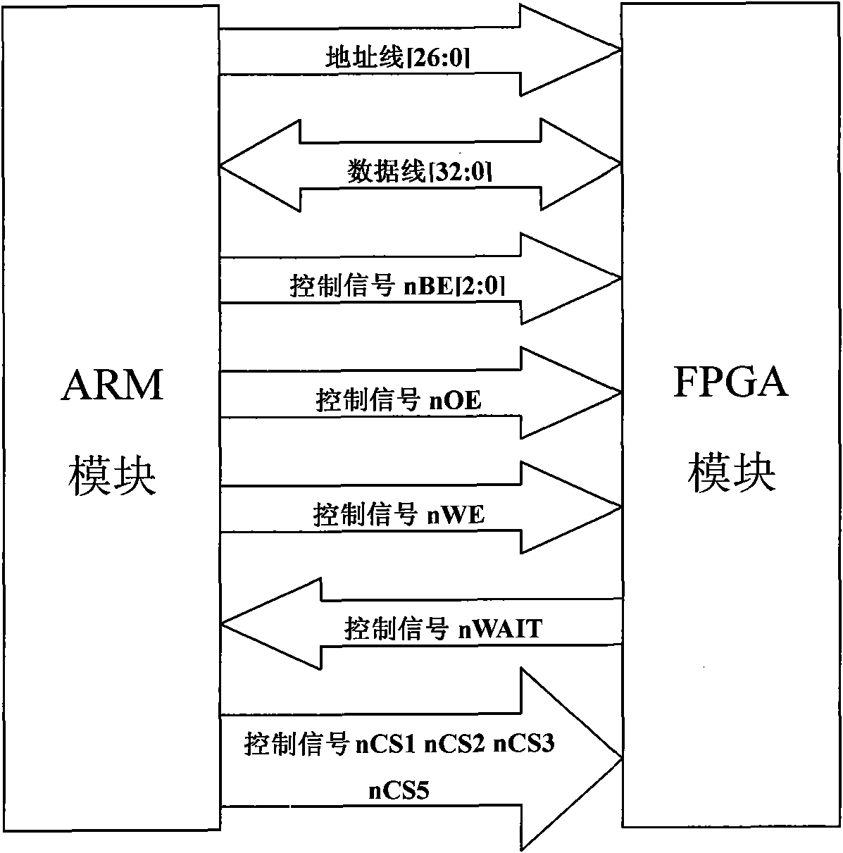
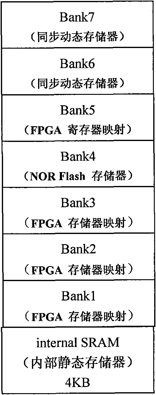
[0025] The invention consists of two modules: ARM module and FPGA module. The two modules are connected by a bus (the FPGA end imitates SRAM memory), and the FPGA end simulates the SRAM external memory, and the FPGA internal controller logic is mapped to the ARM memory to provide data and control access interfaces. Because the access characteristics of various memories are different, the ARM and FPGA communication part adopts a full bus connection, that is, all data lines, address lines, and control lines are all connected to FPGA. Such as figure 1 The overall architecture diagram of the system is shown.

[0026] (1), ARM module

[0027] The ARM module adopts Samsung S3C2440Mobile MCU as the system controller. This MCU is based on the M920T core, has rich on-chip peripherals, supports EBI (External Bus Interface), and provides conditions for FPGA communication. It can run Linux and Windows CE operating systems, providing popular application platform support for the entire v...


PUM


Abstract

The invention discloses a multi-interface memory verification system based on an FPGA, which comprises an ARM module and an FPGA module, wherein the ARM module and the FPGA module are connected in a bus mode, a method of simulating an SRAM external memory through the FPGA end is adopted for logically mapping a controller in the FPGA into the ARM memory for providing data and a control visit interface, the system adopts an asynchronous bus communication mode, asynchronous control signals, asynchronous addresses, and data signals output by the ARM are synchronized to an internal clock region of the FPGA, and the system memory data and the control interface uniformly adopt the direct mapping method of the memory data, so a controller IP core of each memory is transplanted and integrated in the system, and the data visit interface is realized in an FIFO mode. The invention can flexibly support memories with the newest interface types, the newest memory chip can be tested and verified in the shortest time, at the same time, various kinds of chip test and demonstration can be carried out, and the actual use time period of the novel memory chip is greatly shortened.

Description

technical field [0001] The invention relates to the technical fields of communication technology, automatic control and instrumentation, in particular to a field-programmable gate array (FPGA)-based multi-interface memory verification system integrating drive and test of various memories. Background technique [0002] With the introduction of large-capacity and high-speed memories on the market, the increase in capacity and speed has led to differences in the details of the memory and the standard interface. The introduction of new types of memory has fundamentally changed the access interface of the memory and the operation of accessing it. However, mainstream controllers in the market cannot fully support direct access operations to such large-capacity, high-speed memories with special access interfaces. [0003] At present, the mainstream test method of memory at home and abroad is still to test the chips of a single model or a single interface separately. There is no uni...

Claims


Application Information

Patent Timeline
IPC IPC(8): G11C29/56
Inventor 韩定定石山钟慧敏杨晓葛勇张立为
Owner EAST CHINA NORMAL UNIV
Learn More