

Process module facility
A technology of process modules and facilities, applied in metal material coating process, ion implantation plating, gaseous chemical plating, etc., can solve the problems of the bottleneck of the second film layer, difficulty in large substrate transmission and use, complex mechanical design, etc.
- Summary
- Abstract
- Description
- Claims
- Application Information
AI Technical Summary
Problems solved by technology
Method used
Image

Examples
Embodiment Construction
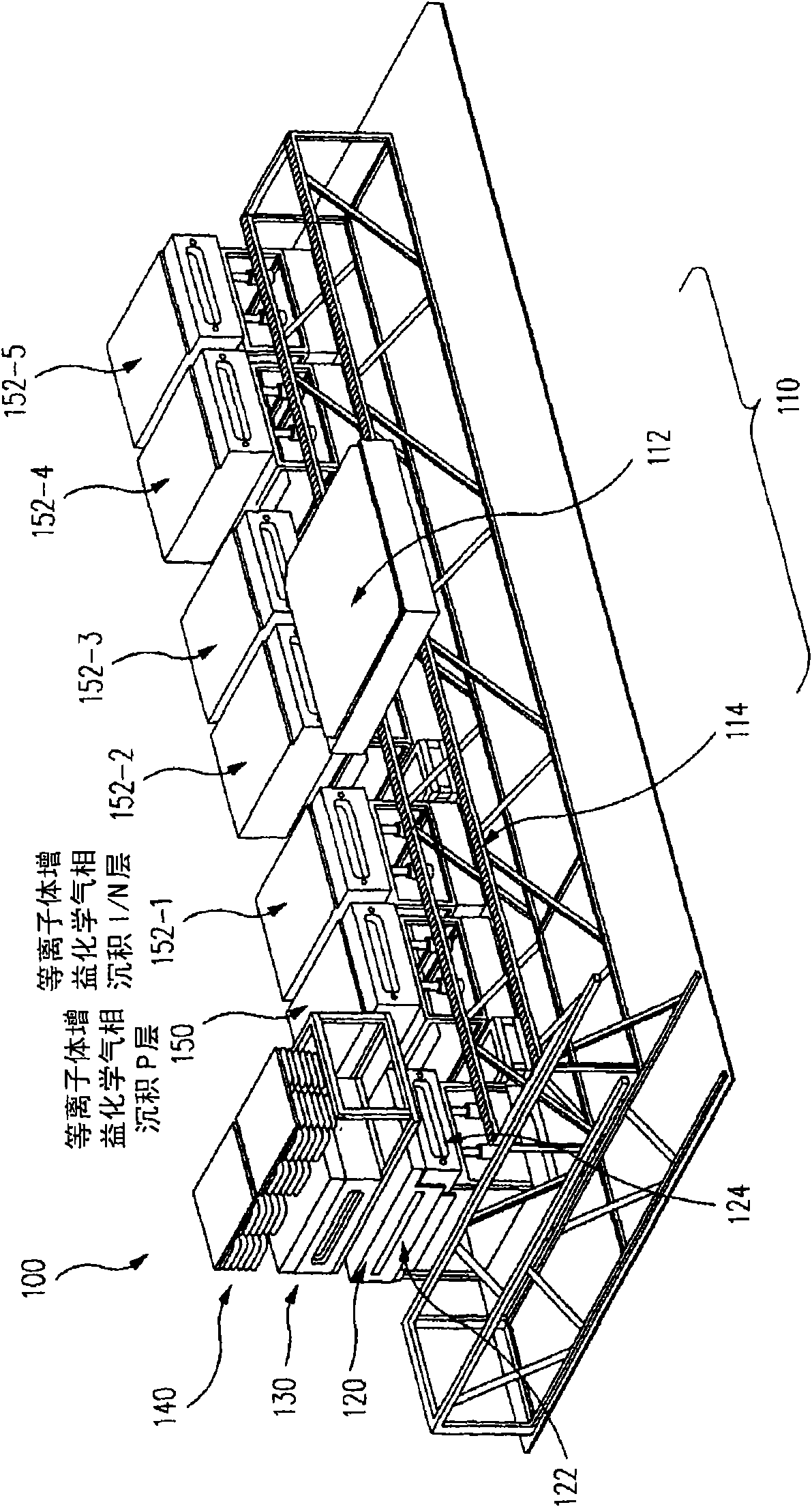
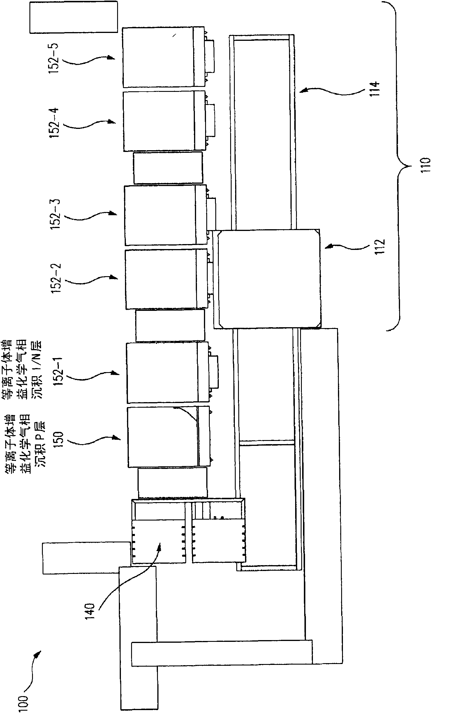
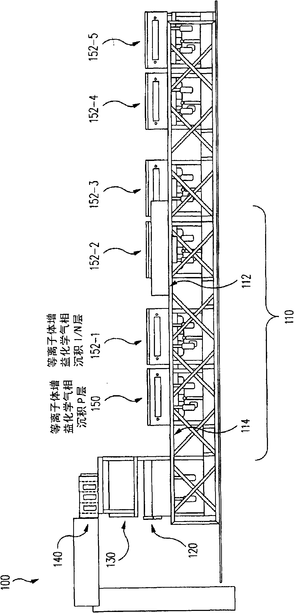
[0052] In general, embodiments described herein relate to systems and methods of processing boards, such as glass and other substrates for the solar or photovoltaic industries, and wafers for the semiconductor industry, but the invention is not limited thereto. More particularly, some embodiments described herein relate to systems and methods for processing substrates that include one or more mobile transverse chambers for transporting substrates between process modules and other stations, such as loading and unloading stations.
[0053] In some embodiments, a system for processing a substrate is provided, comprising: one or more mobile transverse chambers for moving between two or more process modules, and transporting one or more substrates to the two or more process modules at least one of the . Each mobile transverse chamber independently maintains a specific gas condition while moving between process modules and when one or more substrates are transported to the process m...
PUM
 Abstract
Description
Claims
Application Information