Poly(p-phenylene benzobisoxazole) fiber surface-processing method

A technology of benzobisoxazole and polyparaphenylene, which is applied in the direction of electrical components, semiconductor/solid-state device manufacturing, circuits, etc., can solve problems such as reducing the performance of integrated circuits, and achieve the improvement of Avoid the effect of excessive leakage current

Active Publication Date: 2011-10-05
SEMICON MFG INT (SHANGHAI) CORP
View PDF5 Cites 0 Cited by
  • Summary
  • Abstract
  • Description
  • Claims
  • Application Information

AI Technical Summary

Problems solved by technology

[0012] However, compared with other passivation materials such as PI and BCB, PBO has a stronger ability to adsorb metal electrons, so the above-mentioned ashing treatment to reduce the leakage current cannot solve the problem that the leakage current of the PBO passivation layer 11 is too large and reduces the integrated circuit. performance problem

Method used


Image

  • Poly(p-phenylene benzobisoxazole) fiber surface-processing method
  • Poly(p-phenylene benzobisoxazole) fiber surface-processing method
  • Poly(p-phenylene benzobisoxazole) fiber surface-processing method

Examples


Embodiment 1

[0037] Taking the etched sputtered metal layer 22 as the UBM layer as an example, in the bump formation process without the RDL layer, refer to Figure 4A ~ 4I , is a schematic structural diagram of the bump processing process according to the first embodiment of the present invention. The implementation process of steps a1~a4 can be but not limited to:

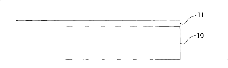
[0038] refer to Figure 4A , providing a semiconductor substrate 40 on which a metal pad layer 41 has been formed;

[0039] The semiconductor substrate 40 is a substrate with semiconductor devices, and for simplicity, it is represented as a blank semiconductor substrate here; corresponding to step a1, the base body 20 is composed of the semiconductor substrate 40 and the metal pad layer 41 at this time.

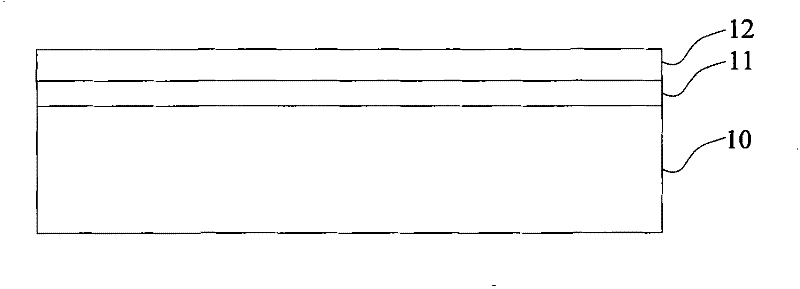
[0040] refer to Figure 4B , form a PBO passivation layer 42 on the semiconductor substrate 40 and the metal pad layer 41, the metal pad layer 41 is embedded in the PBO passivation layer 42, and the metal pad is exposed t...

Embodiment 2

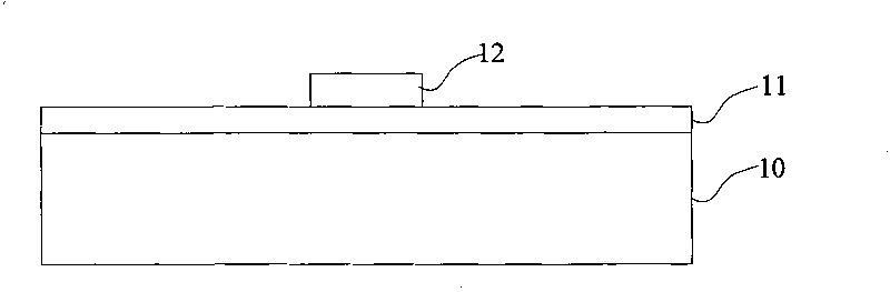
[0053] If the formation of the RDL layer is included in the bump formation process, when the PBO passivation layer is formed, and then the metal corresponding to the RDL layer is sputtered on the PBO passivation layer, the RDL layer can be etched after subsequent photolithography and other processes. After the PBO passivation layer under the RDL layer is exposed, the exposed PBO passivation layer is etched with argon ions, so as to reduce the leakage current in the PBO passivation layer. The etching time may refer to the data in the first embodiment above. Combining with the currently disclosed technology including the RDL layer process flow, it is easy to deduce the implementation process of the second embodiment, which will not be repeated here.


PUM

PropertyMeasurementUnit
thicknessaaaaaaaaaa
thicknessaaaaaaaaaa
thicknessaaaaaaaaaa

Abstract

The invention provides a PBO surface-processing method in order to reduce the leakage current in PBO with the surface splashed with metal and improve the performance of an integrated circuit. The method uses argon ions to etch the PBO surface splashed with metal.

Description

technical field [0001] The invention relates to the field of semiconductor manufacturing, in particular to a surface treatment method for poly-p-phenylene benzobisoxazole fibers (PBO, Poly-P-phenylene-2, 6-benzobisoxazole). Background technique [0002] Based on unique physical properties such as good mechanical tensile and fracture strength, PBO is widely used as a passivation material in integrated circuit packaging technology. [0003] For the sake of brevity, a common simple application model of PBO used as a passivation layer is given below. This application model is applicable to a variety of processes, such as under bump metal layer (UBM) or redistribution layer (RDL) in bump formation process production etc. [0004] Figure 1A ~ 1C It is a schematic diagram of the structure of the existing PBO used as a passivation layer. Combined with this figure, the process of using PBO as a passivation layer is usually: [0005] refer to Figure 1A , first depositing a PBO la...

Claims


Application Information

Patent Timeline
Patent Type & Authority Patents(China)
IPC IPC(8): H01L21/311H01L21/60
Inventor 何智清王重阳章国伟梅娜佟大明
Owner SEMICON MFG INT (SHANGHAI) CORP
Why Eureka
Try Eureka