Organic electroluminescence device
An electroluminescent device, organic technology, applied in the direction of electric solid devices, electrical components, semiconductor devices, etc., can solve the problems of easy falling off, device pollution, metal deformation, etc., to expand the selection range, overcome poor adhesion, and solve easy peeling. Effect
- Summary
- Abstract
- Description
- Claims
- Application Information
AI Technical Summary
Problems solved by technology
Method used
Image
Examples
Embodiment 1
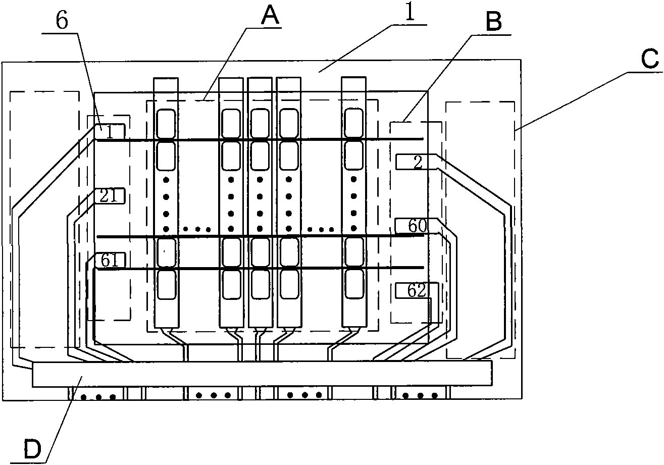
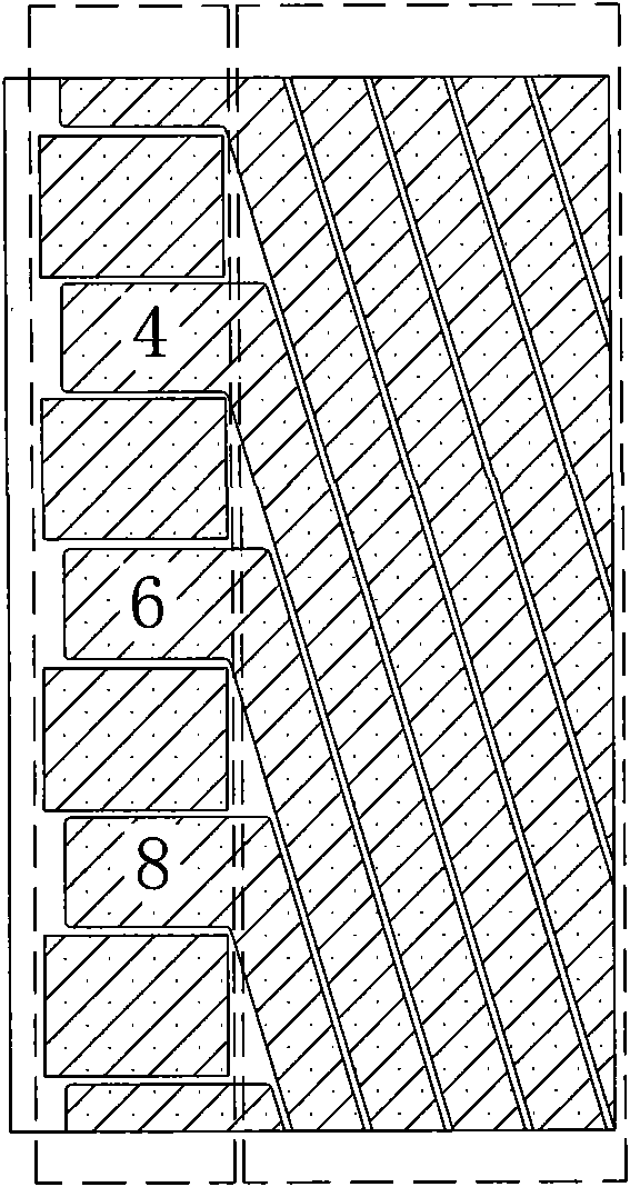
[0035] refer to image 3 . The organic electroluminescent device in this embodiment includes a substrate, an anode strip, an organic functional layer, and a cathode strip. The substrate is divided into a light-emitting area and a lead area, and a metal mounting area where the cathode strip and its lead are overlapped is set between the light-emitting area and the lead area. The embodiment is that odd-numbered rows and even-numbered rows of metal mounting areas are separately set up on the left and right sides of the screen body, refer to Figure 3-a , just take the metal mounting area on the right as an example. The insulating layer is located in even-numbered rows such as 4, 6, and 8. On the layer (ITO), the pattern on the right edge of the insulating layer forms a comb-like shape. The loading positions of even-numbered rows such as 4, 6, and 8 are the conductive layer (ITO), the low-resistance metal layer (chromium or molybdenum or molybdenum-aluminum-molybdenum), and the ...
Embodiment 2
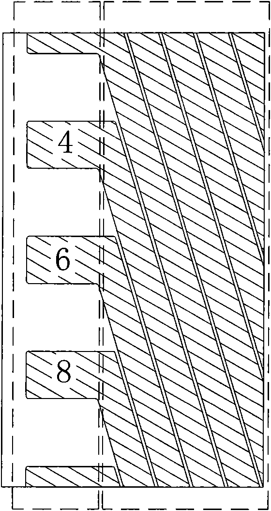
[0037] refer to Figure 4 . The organic electroluminescent device in this embodiment includes a substrate, an anode strip, an organic functional layer, and a cathode strip. The substrate is divided into a light-emitting area and a lead area, and a metal mounting area where the cathode strip and its lead are overlapped is set between the light-emitting area and the lead area. The embodiment is that odd-numbered rows and even-numbered rows of metal mounting areas are separately set up on the left and right sides of the screen body, refer to Figure 3-a , only take the metal mounting area on the right as an example, and the insulating layer pattern refers to Figure 3-a ,and Figure 1-b The pattern is the same, the area located above the low-resistance metal rectangular layer, the insulating layer is ring-shaped, and the middle through hole is the real overlapping area between the cathode and the low-resistance metal. Figure 3-b It is a low-resistance metal layer pattern, whi...
Embodiment 3
[0039] refer to Figure 4 . The organic electroluminescent device in this embodiment includes a substrate, an anode strip, an organic functional layer, and a cathode strip. The substrate is divided into a light-emitting area and a lead area, and a metal mounting area where the cathode strip and its lead are overlapped is set between the light-emitting area and the lead area. The embodiment is that odd-numbered rows and even-numbered rows of metal mounting areas are separately set up on the left and right sides of the screen body, refer to Figure 4-a , only take the metal mounting area on the right as an example, and the insulating layer pattern refers to Figure 3-a ,and Figure 1-b The pattern is the same, the area located above the low-resistance metal rectangular layer, the insulating layer is ring-shaped, and the middle through hole is the real overlapping area between the cathode and the low-resistance metal. Figure 4-b It is a low-resistance metal layer pattern, and...
PUM
 Abstract
Description
Claims
Application Information


