Manufacturing method of novel printed circuit board

A technology of printed circuit board and manufacturing method, which is applied in the direction of electrical connection formation of printed components, etc., can solve the problems of poor thermal reliability performance, poor bonding force between conductive layer and dielectric layer, etc.

Active Publication Date: 2010-07-28
SHANGHAI MEADVILLE SCI & TECH
View PDF1 Cites 26 Cited by
  • Summary
  • Abstract
  • Description
  • Claims
  • Application Information

AI Technical Summary

Problems solved by technology

[0012] The purpose of the present invention is to provide a novel method of manufacturing printed circuit boards in view of the above-mentioned defects in the prior art, which is different from the process of electroplating and filling holes on the entire board surface commonly used in the circuit board industry, and proposes a pattern electroplating process. Hole filling process, that is, complete blind hole electroplating while completing conductor growth, and blind holes are filled by electroplating to form solid conductive columns; at the same time, the present invention uses an improved semi-additive process to make fine lines. Among them, the conductive layer on the dielectric layer is formed by thermocompression, so it can effectively avoid the problems of poor bonding force between the conductive layer and the dielectric layer and poor thermal reliability.

Method used


Image

  • Manufacturing method of novel printed circuit board
  • Manufacturing method of novel printed circuit board
  • Manufacturing method of novel printed circuit board

Examples


Embodiment Construction

[0046] The manufacturing method of the present invention will be further described below in conjunction with the accompanying drawings.

[0047] see Figure 5a ~ Figure 5h , the present invention adopts the improved semi-additive method to combine with the hole-filling process under pattern electroplating to manufacture the concrete steps of the printed circuit board as follows:

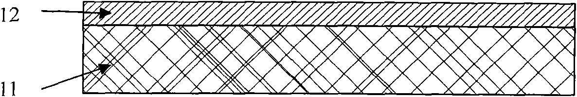
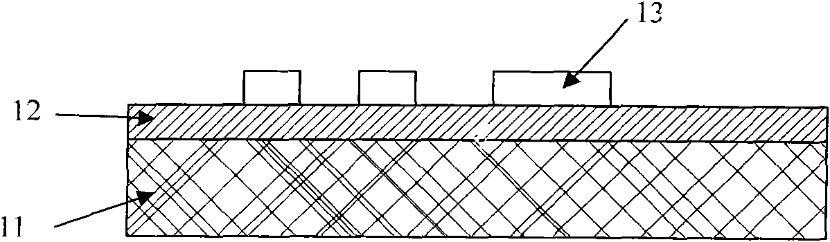
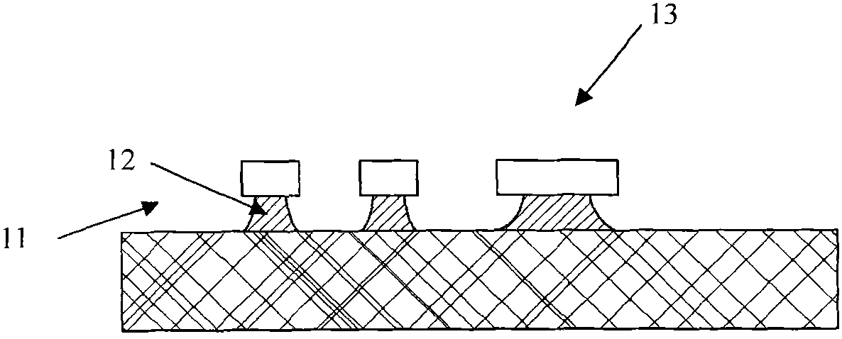
[0048] Step 1, such as Figure 5a As shown, first a dielectric layer 52 is prepared, and a conductive layer 51 is thermally pressed on the dielectric layer. The dielectric layer can be fabricated on a composite substrate including an insulating carrier and a surface conductive layer, or can be directly fabricated on the conductive layer. In this embodiment, the dielectric layer 52 and the conductive layer 51 are laminated and formed on the substrate 53 including the dielectric layer and the conductive layer. The dielectric layer 52 is epoxy resin material containing glass cloth, and the conductive...


PUM


Abstract

The invention relates to a manufacturing method of a novel printed circuit board, which can form fine circuits and laminated interconnection based on the improved semi-additive process and the process of pore filling under pattern plating. The specific steps of the method are as follows: a) preparing a dielectric layer and laminating a conductive layer on the dielectric layer, thereby forming a substrate of a composite structure with the dielectric layer and the conductive layer; b) manufacturing conduction blind holes on the dielectric layer and the conductive layer; c) carrying out conduction treatment for the conductive layer and the walls of the conduction blind holes, thereby forming a seed layer; d) adhering a light-sensitive film to the surface of the substrate and forming a plated blocking layer on the substrate through pattern transfer; e) plating the substrate with the plated blocking layer, forming a conductor pattern, and filling the conduction blind holes through plating, thereby forming a solid conductive pole; f) removing the plated blocking layer; g) removing the exposed seed layer and the conductive layer below the seed layer, and reserving the conductor pattern and circuits formed through plating, thereby forming a circuit board; and h) repeating the steps from Step a) to Step g) on the circuit board, so as to realize the multi-layer superposition.

Description

technical field [0001] The invention relates to a novel method for manufacturing a printed circuit board, specifically a method for realizing interlayer interconnection based on pattern electroplating and hole filling, and a method for forming fine circuits by using an improved semi-additive method. Background technique [0002] With the development of electronic products in the direction of thinner and smaller, the requirements for product refinement are getting higher and higher. In the production of printed circuit boards, in addition to reducing the diameter of the via hole, reducing the size of the circuit is also an important direction to increase product density and reduce the size of the completed board. [0003] At present, in the circuit board manufacturing process, three typical pattern transfer technologies are: subtractive method, full additive method and semi-additive method. In the ordinary subtractive process, a photosensitive resist material is generally us...

Claims


Application Information

Patent Timeline
Patent Type & Authority Applications(China)
IPC IPC(8): H05K3/42
Inventor 任潇璐付海涛程凡雄罗永红陈培峰
Owner SHANGHAI MEADVILLE SCI & TECH
Why Eureka
Try Eureka