
Multiband matching circuit and multiband power amplifier

A matching circuit and multi-band technology, applied to power amplifiers, improved amplifiers to reduce temperature/power supply voltage changes, electrical components, etc., can solve problems such as loss deterioration, and achieve the effect of reducing current flow and low loss

Inactive Publication Date: 2010-08-04
NTT DOCOMO INC
View PDF0 Cites 7 Cited by
  • Summary
  • Abstract
  • Description
  • Claims
  • Application Information

AI Technical Summary

Problems solved by technology

Such a problem of worsened pass loss occurs similarly when a reactance element or a reactance circuit is used instead of the series connection of the switch and the sub-matching block.

Method used


Image

  • Multiband matching circuit and multiband power amplifier
  • Multiband matching circuit and multiband power amplifier
  • Multiband matching circuit and multiband power amplifier

Examples


Embodiment 1

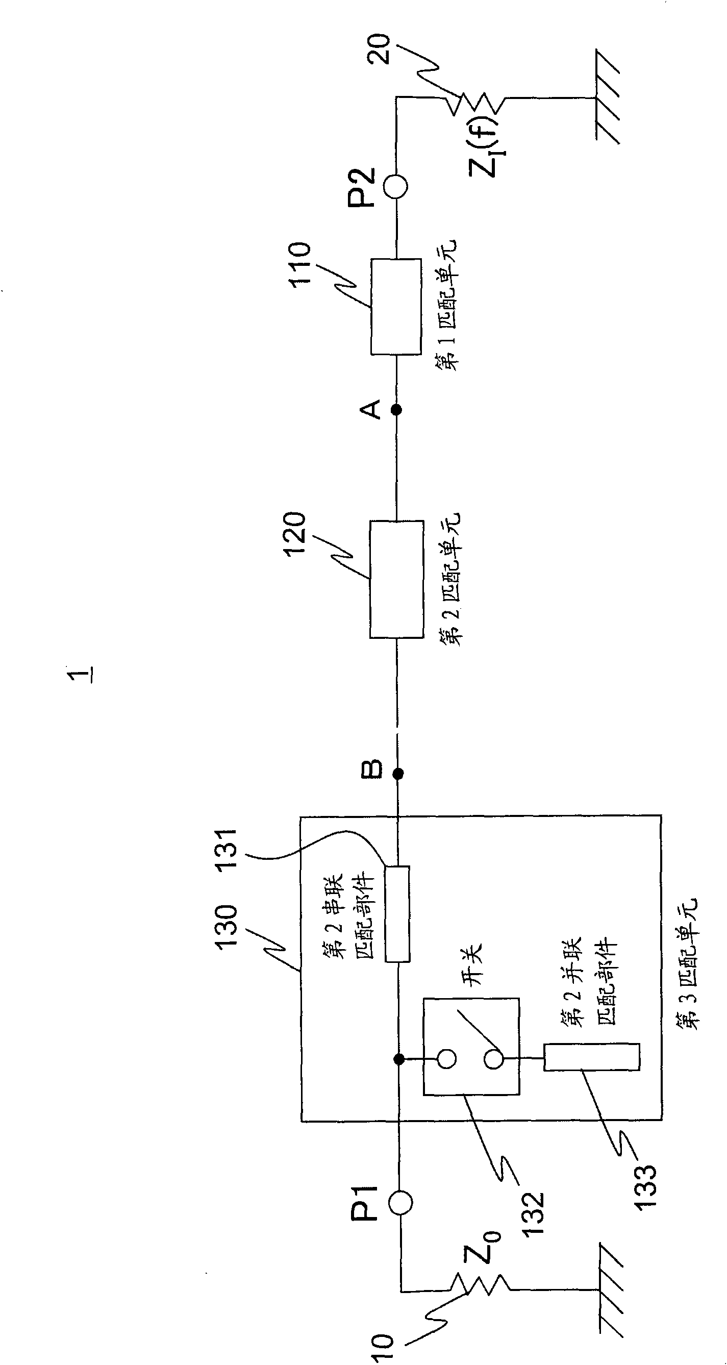
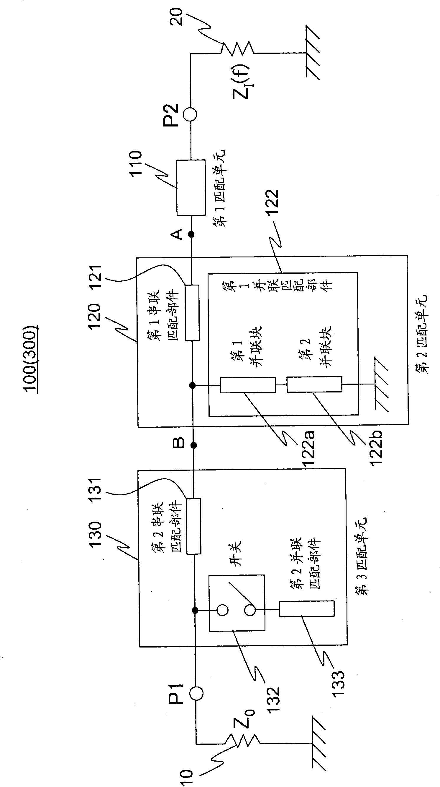
[0067] First, before describing the embodiments, the principle of reducing the amount of current flowing through the switch according to the present invention will be described. figure 1 The basic configuration of the matching circuit of the present invention is shown. The matching circuit 1 of the basic structure adopts the following structure: the second matching unit 120 is further added between the first matching unit 110 corresponding to the main matching block 310 of the matching circuit 300 and the third matching unit 130, wherein the third matching unit 130 corresponds to a group of the delay circuit 321 and the switch 322 and the sub-matching block 323 of the matching circuit 300 . The second matching unit 120 is wrong b 1 The matching in brings influence, will b 2 Z(f in 2 ) is transformed into the impedance Z′(f 2 ). b 2 The matching in is realized by the third matching unit 130. Also, the current flowing through the switch 132 of the third matching unit 130...

Embodiment 2

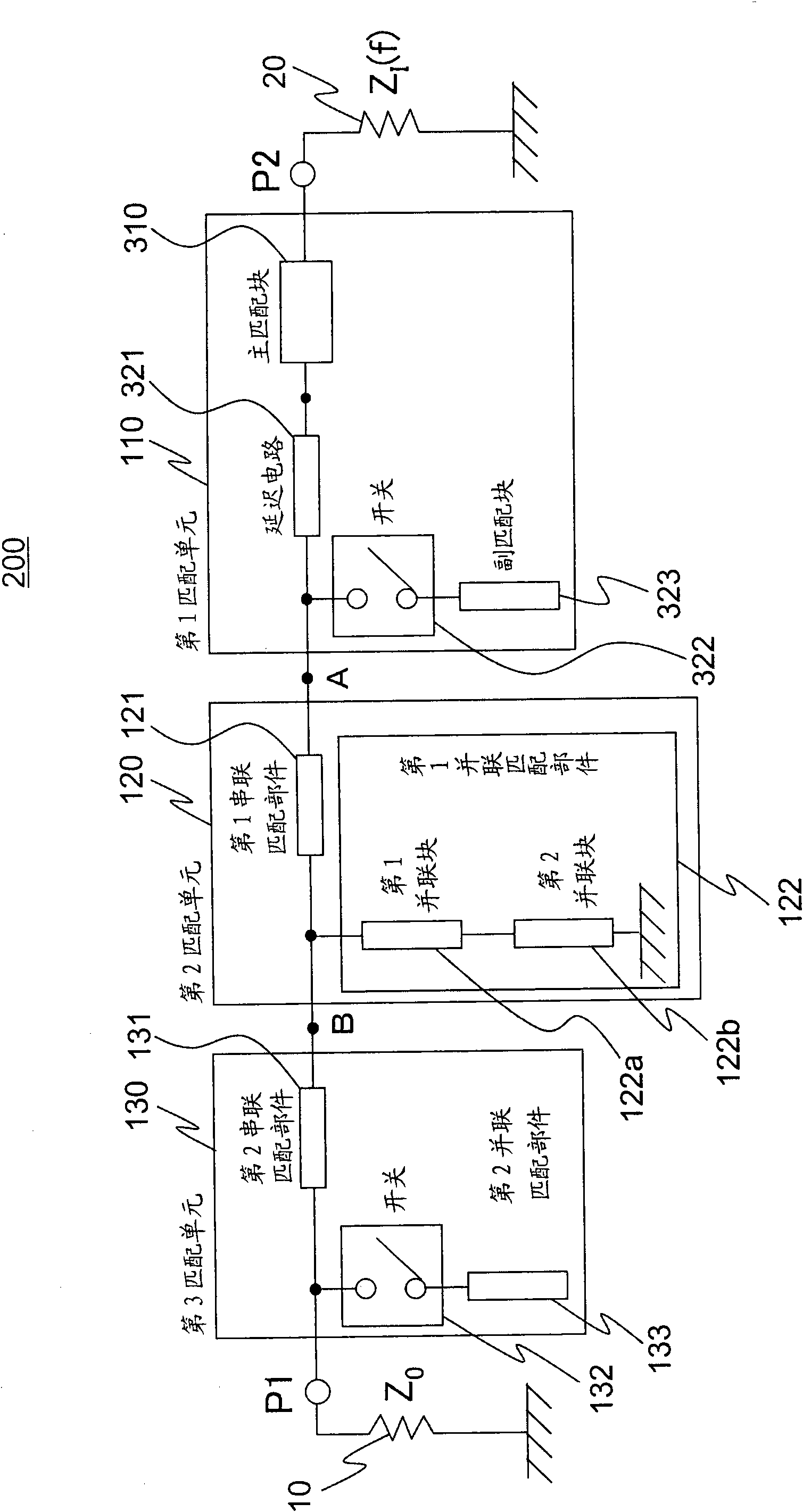
[0098] image 3 The matching circuit 200 of the second embodiment is shown. The matching circuit 200 is for the figure 2 The configuration of the matching circuit 300 described as background art is applied to the first matching section 110 of the matching circuit 100 according to the first embodiment shown. The first matching unit 110 selectively connects the circuit element 20 at b by switching the switch 322 1 The impedance Z in I (f 1 ) and b 2 The impedance Z in I (f 2 ) to Z 0 . That is, from image 3 Point A looks towards b on the side of P2 1 The impedance in the OFF state of switch 322 becomes Z 0 , b 2 The impedance in the ON state of switch 322 becomes Z 0 . And, when the switch 132 is in the OFF state, in the first matching unit 110 according to the state of the switch 322, b 1 or b 2 The matching state obtained by any one of the (impedance Z 0 ), even if it passes through the second and third matching units, it is maintained as it is, and as a who...

Embodiment 3

[0108] figure 2 In the first matching unit 110 of the matching circuit 100 of the shown embodiment 1, in addition to the structure listed in the second embodiment, the matching circuit 100 can also be applied therein, or the signal matching of three or more frequency bands can be applied. any matching circuit.

[0109] When a matching circuit capable of matching multiple or one of three or more (m-1) frequency bands is applied to the first matching unit 110, the first to second frequency bands can be configured by turning on and off the switch 132. Multiple or one of m-1 frequency bands and m-th frequency band b m (center frequency f m ) in a matching circuit 300 that can be selectively matched (refer to figure 2 ). At this time, the first matching unit 110 sets the circuit element 20 at b 1 to b m-1 The impedance Z in I (f 1 ),Z I (f 2 ),...,Z I (f m-1 ) into Z 0 . And, when the switch 132 is in the OFF state, in the first matching unit 110 about b 1 to b m-...


PUM


Abstract

The present invention relates to a multiband matching circuit and a multiband power amplifier, including a first matching unit, a second matching unit, and a third matching unit. Matching with target impedance is established at a first frequency by appropriately designing the first matching unit and at a second frequency by appropriately designing the second and third matching units. The second matching unit and the third matching unit are designed to make the conversion ratio of the impedance viewed from the connection point between the second matching unit and the third matching unit to a circuit element to the target impedance smaller than the conversion ratio of the impedance viewed from the connection point between the first matching unit and the second matching unit to the circuit element to the target impedance, at the second frequency.

Description

technical field [0001] The present invention relates to matching circuits for amplifiers and the like, and power amplifiers. More specifically, it relates to low loss in a multiband matching circuit capable of establishing matching between input and output impedances of circuit elements having frequency characteristics such as amplifier elements and characteristic impedances of peripheral circuits in multiple frequency bands. Background technique [0002] It is required that a wireless device can handle signals of multiple frequency bands (multi-band). As an indispensable device included in a wireless device, there is a power amplifier. In order to perform high-efficiency amplification, it is necessary to be able to adjust the input and output impedances of amplifying elements (transistors, etc.) I (f), set the output impedance to Z L (f)) and the input and output impedance Z of the peripheral circuit 0 (=system impedance) is a multi-band matching circuit that matches th...

Claims


Application Information

Patent Timeline
Patent Type & Authority Applications(China)
IPC IPC(8): H03F3/20H03F1/30
CPCH03H7/383H03H7/38H03H2007/386
Inventor 福田敦史冈崎浩司楢桥祥一
Owner NTT DOCOMO INC
Learn More