Phase change memory chip layout structure

A phase change memory and layout structure technology, applied in the field of microelectronics, can solve the problems of signal distortion, read and write data errors, etc., and achieve the effect of reducing interference and reasonable chip layout.

Active Publication Date: 2010-08-11
SHANGHAI INST OF MICROSYSTEM & INFORMATION TECH CHINESE ACAD OF SCI
View PDF0 Cites 3 Cited by
  • Summary
  • Abstract
  • Description
  • Claims
  • Application Information

AI Technical Summary

Problems solved by technology

Among them, the voltage-controlled oscillator in the phase-locked loop has oscillation noise, and other digital circuits will also introduce digital noise. If these noises interfere with the analog circuit and the storage array, it will cause signal distortion and read and write data errors.

Method used


Image

  • Phase change memory chip layout structure
  • Phase change memory chip layout structure
  • Phase change memory chip layout structure

Examples


Embodiment 1

[0022] The invention discloses a phase-change memory chip layout structure, which makes the layout of the chip layout more reasonable.

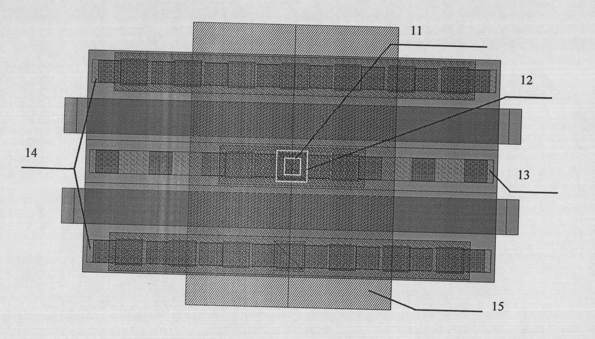
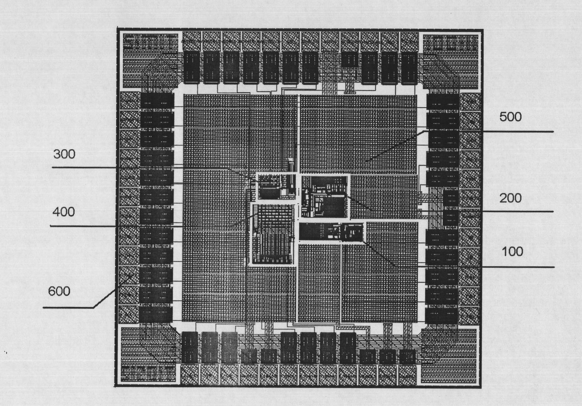
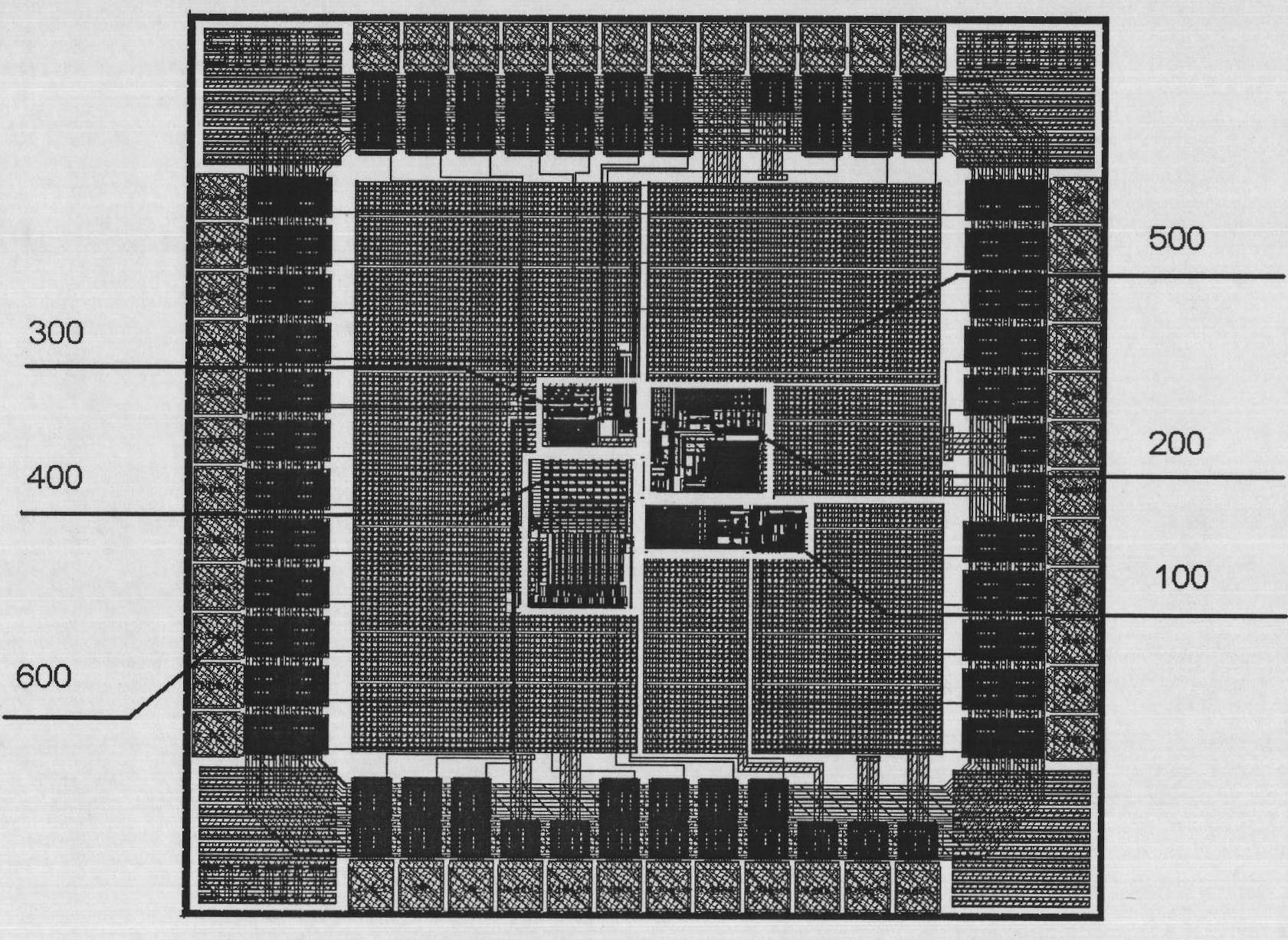
[0023] see figure 2 , this embodiment takes a phase-change memory with a capacity of 512 bits manufactured by a 180nm CMOS process as an example to illustrate the layout structure of a phase-change memory chip provided by the present invention. The phase change memory chip layout is composed of a first layout area 100, a second layout area 200, a third layout area 300, a fourth layout area 400, a fifth layout area 500 and a sixth layout area 600; the first layout area 100, The second layout area 200, the third layout area 300 and the fourth layout area 400 are located in the center of the phase change memory chip layout; the first layout area 100 is connected to the second layout area 200, and the second layout area 200 is connected to the third layout area 300 The second layout area 200 is connected to the fourth layout area 400, the third...


PUM


Abstract

The invention discloses a phase change memory chip layout structure. A phase change memory chip layout comprises a first layout area, a second layout area, a third layout area, a fourth layout area, a fifth layout area and sixth layout areas, wherein the first layout area, the second layout area, the third layout area and the fourth layout area are positioned in the center of the phase change memory chip layout; the first layout area is connected with the second layout area; the second layout area is connected with the third layout area and the fourth layout area; the third layout area is connected with the fourth layout area; the fifth layout area covers other blank areas in the center of the layout except the first layout area, the second layout area, the third layout area and the fourth layout area; and the sixth layout areas are uniformly distributed on four sides and four corners of the phase change memory chip layout. The phase change memory chip layout structure has reasonable chip layout and effectively reduces the noise of a voltage-controlled oscillator and the disturbance of the noise of a digital circuit on an analog circuit and a storage array.

Description

technical field [0001] The invention belongs to the technical field of microelectronics and relates to a chip layout structure, in particular to a phase change memory chip layout structure. Background technique [0002] Phase change memory technology has great development prospects, and has the advantages of fast read and write speed, high density, low power consumption, low cost, non-volatility, high resistance to repeated erasing and writing, and compatibility with CMOS technology. Phase change memory utilizes the difference in electrical conduction characteristics of phase change materials when they switch between crystalline and amorphous states to store data. The phase change material is in a low-resistance state in the crystalline state, called the set state, representing "0"; in the amorphous state, it is in a high-resistance state, called the reset state, representing "1". [0003] Phase change materials are mostly chalcogenide amorphous semiconductor materials, suc...

Claims


Application Information

Patent Timeline
Patent Type & Authority Applications(China)
IPC IPC(8): H01L27/24
Inventor 王倩陈后鹏蔡道林宋志棠
Owner SHANGHAI INST OF MICROSYSTEM & INFORMATION TECH CHINESE ACAD OF SCI
Why Eureka
Try Eureka