Buried low-resistance metal word lines for cross-point variable-resistance material memories

A resistance material and memory technology, applied in the field of variable resistance material random access memory, can solve the problems of complex memory unit size and processing complexity

Active Publication Date: 2010-08-11
MICRON TECH INC
View PDF2 Cites 8 Cited by
  • Summary
  • Abstract
  • Description
  • Claims
  • Application Information

AI Technical Summary

Problems solved by technology

This wire bonding can also lead to further complicating the memory cell size and processing complexity

Method used


Image

  • Buried low-resistance metal word lines for cross-point variable-resistance material memories
  • Buried low-resistance metal word lines for cross-point variable-resistance material memories
  • Buried low-resistance metal word lines for cross-point variable-resistance material memories

Examples


Embodiment Construction

[0018] Embodiments of devices, devices, or articles described herein can be manufactured, used, or shipped in a variety of orientations and orientations. Variable resistance material memory devices may include materials such as alloys. Variable resistance material memory devices may include materials such as metalloid components. Variable resistance material memory devices may include materials such as metal oxides. Variable resistance material memory devices may include materials such as chalcogenides. These several materials can vary widely in quality and performance.

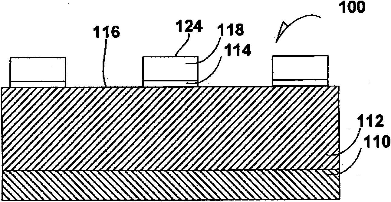
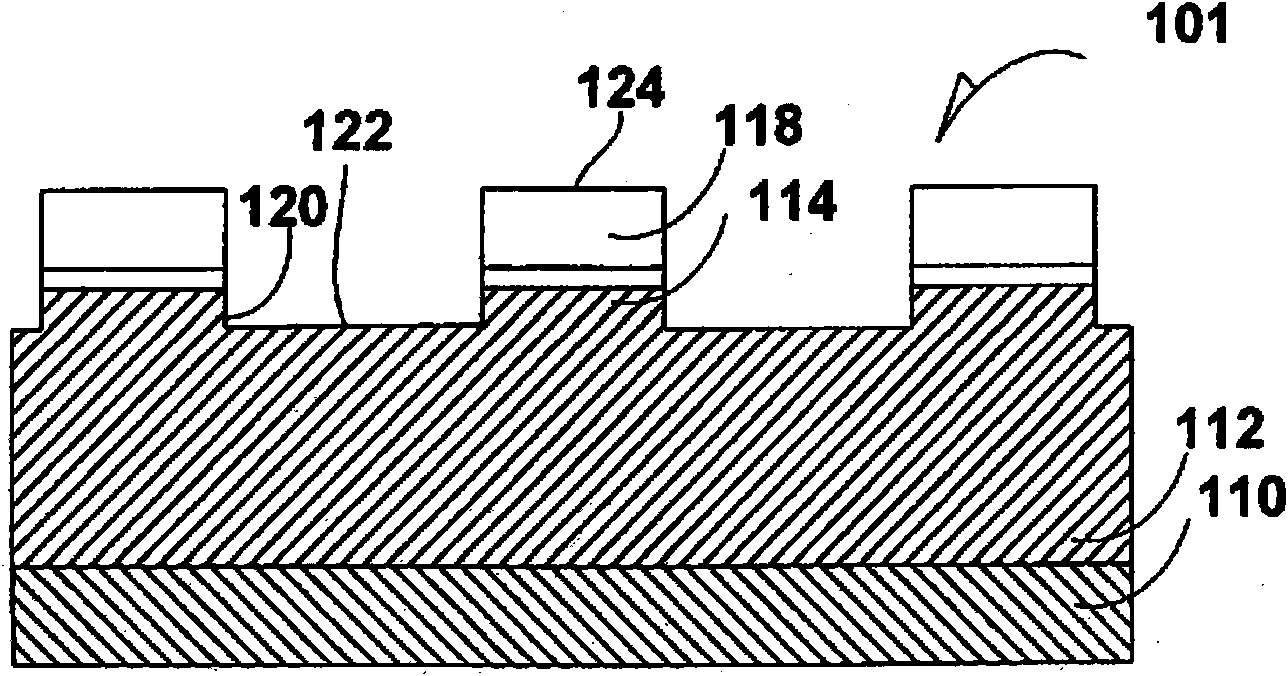
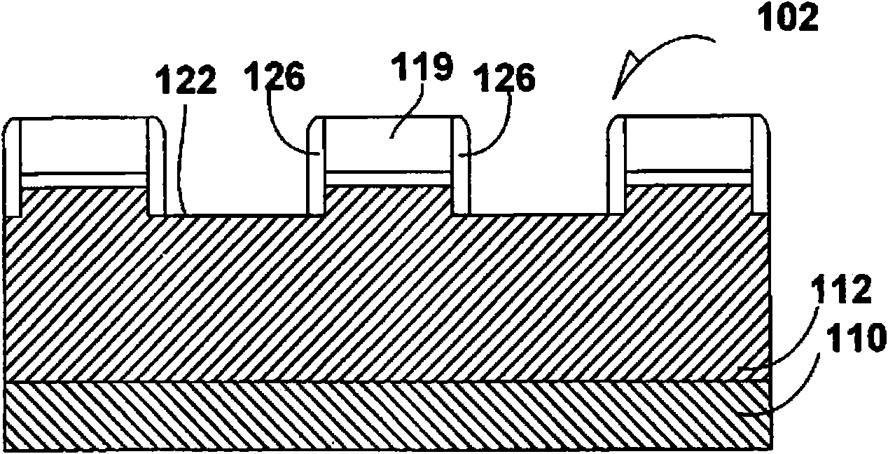
[0019] Figure 1a A cross-sectional front view of a semiconductor device 100 during processing according to an embodiment is shown. A semiconductive lower substrate 110 has been formed below a semiconductive upper substrate 112 . In an embodiment, the semiconductive lower substrate 110 is P− doped as compared to the N+ doped semiconductive upper substrate 112 .

[0020] A dielectric film 114 , such as s...


PUM


Abstract

Variable-resistance material memories include a buried salicide word line disposed below a diode. Variable-resistance material memories include a metal spacer spaced apart and next to the diode. Processes include the formation of one of the buried salicide word line and the metal spacer. Devices include the variable-resistance material memories and one of the buried salicided word line and the spacer word line.

Description

technical field [0001] The present invention relates generally to variable resistance material random access memories. [0002] This patent application claims priority to US Application Serial No. 11 / 857,682, filed September 19, 2007, which is incorporated herein by reference. Background technique [0003] RRM memory structures typically rely on heavily doped semiconducting leads that act as word lines in cross-point RRM random access memory. Significant parasitic resistive voltage drops can occur in such word lines due to the programming currents used in variable resistive material random access memories. Therefore, back-end metal line bonding can be applied to reduce word line resistance. This metal wire bonding can also lead to further complicating memory cell size and processing complexity. [0004] Methods are now needed to develop better structures that can address these challenges. There is also a need for improved variable resistance material random access memory...

Claims


Application Information

Patent Timeline
Patent Type & Authority Applications(China)
IPC IPC(8): H01L27/115H01L21/8247H10B69/00H10B99/00
CPCH01L27/24H01L27/101H10B63/20H10B63/80H10B63/10H10N70/231H10N70/826H10N70/8828H10N70/8825H10N70/8833H10N70/8836H10N70/20H01L21/28141H01L21/28052G11C13/0004G11C2213/72G11C2213/31G11C2213/75G11C2213/32H10B99/00H10B63/00H10N70/021H10N70/841H10N70/8822
Inventor 刘峻迈克尔·P·瓦奥莱特
Owner MICRON TECH INC
Why Eureka
Try Eureka