NOR type flash memory structure with double ion implantation and manufacturing method thereof

A technology of ion implantation and manufacturing method, which is applied in semiconductor/solid-state device manufacturing, electrical components, electrical solid-state devices, etc. It can solve the problems of serious electrical connection and affecting carrier mobility in flash memory, etc., and achieve long service life, Write and scrub program stable effect

Active Publication Date: 2010-09-08
EON SILICON SOLUTION
View PDF0 Cites 6 Cited by
  • Summary
  • Abstract
  • Description
  • Claims
  • Application Information

AI Technical Summary

Problems solved by technology

In order to avoid the short channel effect, the thinner and thinner the lightly doped drain region will make the fragile electrical connection more and more serious, which will affect the mobility of carriers in the flash memory.

Method used


Image

  • NOR type flash memory structure with double ion implantation and manufacturing method thereof
  • NOR type flash memory structure with double ion implantation and manufacturing method thereof
  • NOR type flash memory structure with double ion implantation and manufacturing method thereof

Examples


Embodiment Construction

[0053] In order to fully understand the purpose, features and effects of the present invention, the present invention will be described in detail through the following specific embodiments and accompanying drawings, which will be described later. In these different drawings and embodiments, the same components will use the same symbols.

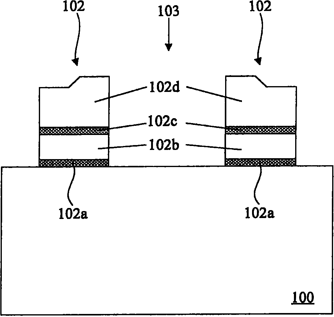
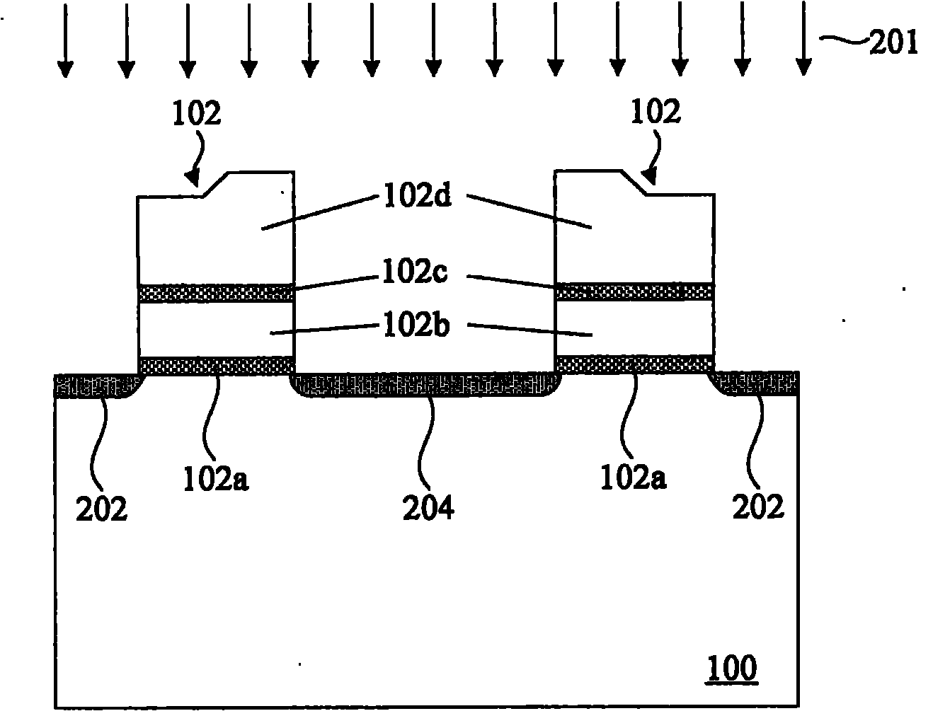
[0054] First refer to figure 1, is a partial cross-sectional view of the flash memory structure of the present invention. The figure shows that two gate structures 102 are formed on a semiconductor substrate 100, and these gate structures 102 respectively include: a tunneling oxide layer 102a (tunneling oxide layer), a floating gate 102b (floating gate), a dielectric layer 102c, A control gate 102d (control gate) forms a channel 103 . The material of the semiconductor substrate 100 can be silicon, silicon germanium (SiGe), silicon on insulator (SOI), silicon germanium on insulator (SGOI), germanium on insulator ( germanium on insulator, G...


PUM


Abstract

The invention provides an NOR type flash memory structure with double ion implantation and a manufacturing method thereof, wherein the NOR type flash memory structure comprises a semiconductor substrate, a lightly doped drain region, a first source region, a highly doped drain region, a phosphorus-doped drain region, two automatic alignment metal silicide layers and a barrier plug. The NOR type flash memory structure can strengthen the electrical connection at the junction of the lightly doped drain region and the highly doped drain region after improving the short channel effect and avoiding the phenomenon that the lightly doped drain region is easy to be dug through when etching, and the mobility of a current carrier in a memory can not be reduced.

Description

technical field [0001] The present invention relates to a NOR flash memory structure and a manufacturing method thereof, in particular to a NOR flash memory (flash memory) structure with double ion implantation and a manufacturing method thereof. Background technique [0002] Flash memory is a kind of non-volatile (non-volatile) memory, that is, it can save information content even when there is no external power supply, which makes the device itself not need to waste power on data storage, and flash memory also has duplication The characteristics of reading and writing, small size, high capacity and portability make flash memory especially suitable for use in portable devices. At present, the scope of NOR-type flash memory application, in addition to the motherboard on the personal computer will use NOR-type flash memory to store BIOS data, mobile phones, handheld devices will also use NOR-type flash memory to store system data, through its high-speed reading speed, meet th...

Claims


Application Information

Patent Timeline
Patent Type & Authority Applications(China)
IPC IPC(8): H01L27/115H01L21/8247H01L21/265H01L27/11521H01L27/11524
Inventor 吴怡德李永忠陈宜秀
Owner EON SILICON SOLUTION
Why Eureka
Try Eureka