Silicon electromagnetic casting device

An electromagnetic casting and voltage technology, applied in the field of silicon electromagnetic casting devices, can solve problems such as increased input power, solidification, and electromagnetic interference, and achieve high-quality, large-volume effects

Active Publication Date: 2010-09-15
丽达科技有限公司 +1
View PDF4 Cites 16 Cited by
  • Summary
  • Abstract
  • Description
  • Claims
  • Application Information

AI Technical Summary

Problems solved by technology

[0005] However, the above-mentioned silicon electromagnetic casting method has the following problems: if in order to improve production efficiency, thereby increasing the volume of the silicon block S, along with the increase of the amount of the silicon block required to be melted, the required input power will also increase
[0010] At the same time, the surface erosion of the crucible 2...

Method used


Image

  • Silicon electromagnetic casting device
  • Silicon electromagnetic casting device
  • Silicon electromagnetic casting device

Examples


Embodiment 1

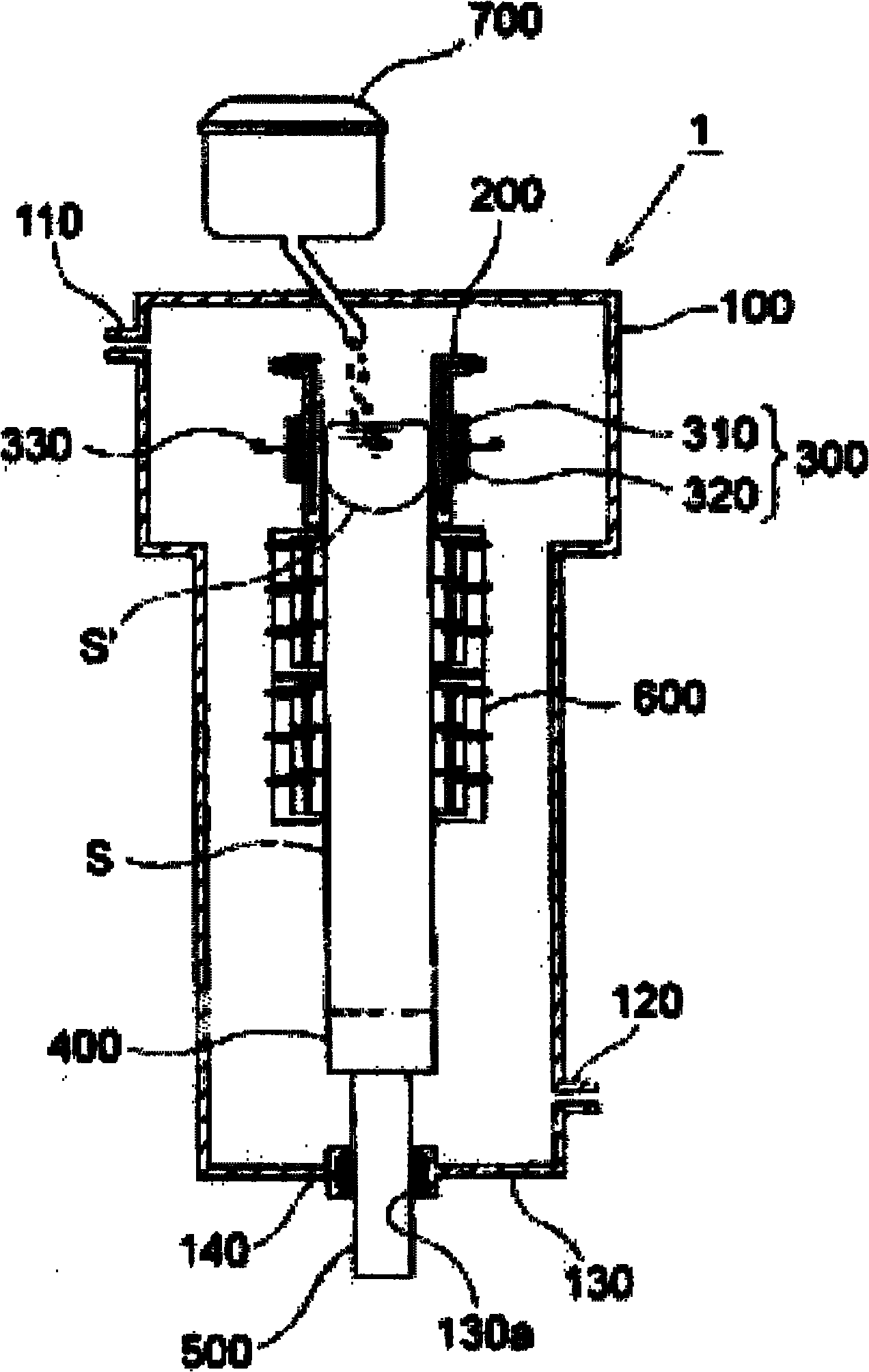
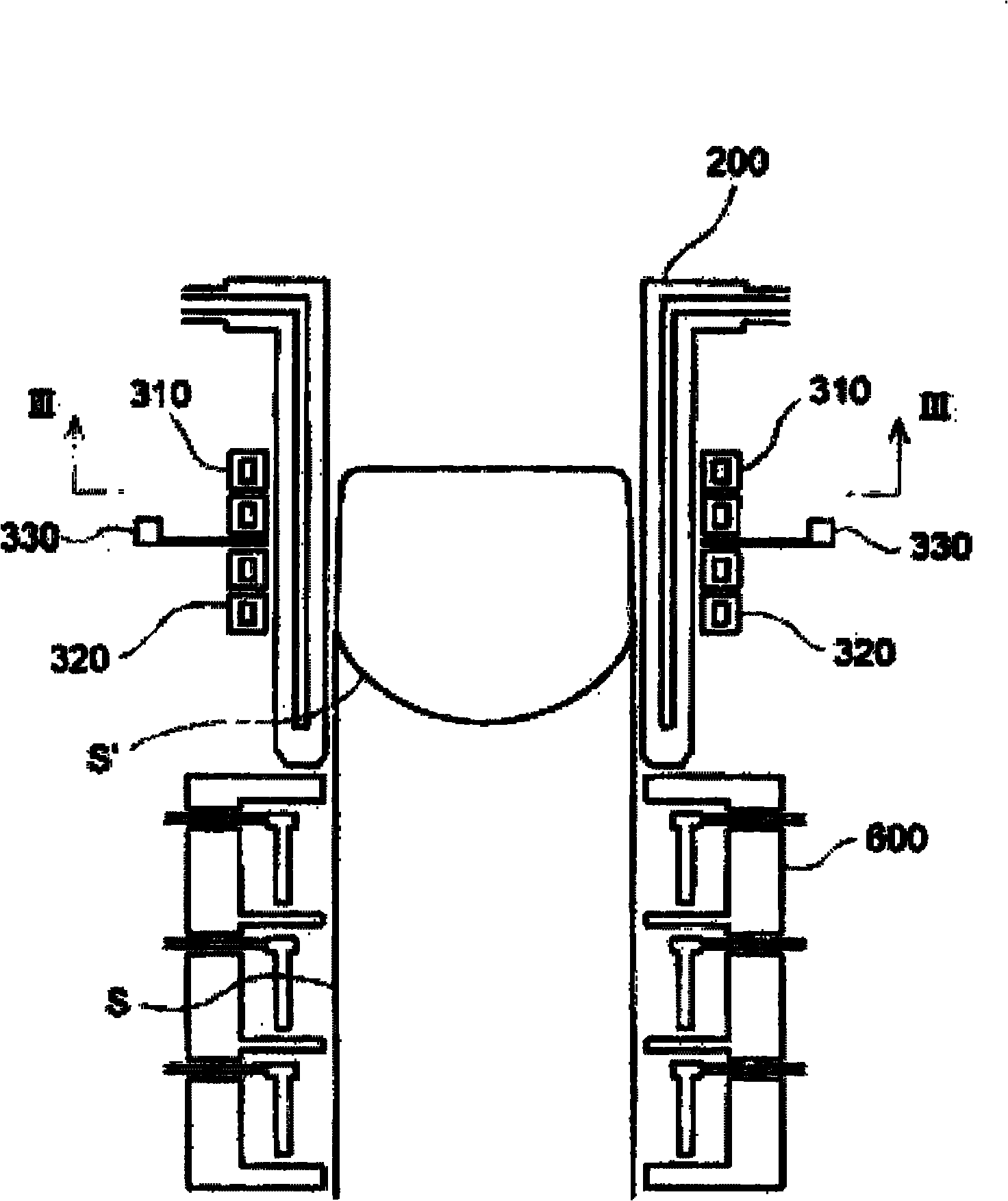
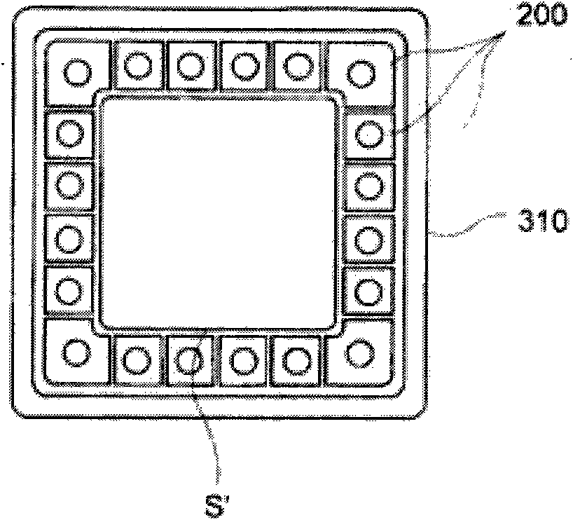
[0074] In this device 1, two induction coils 310, 320 with different induction frequencies are used, and the conductive crucible 200 which is insulated in the vertical direction and has a cooling water circulation inside interacts with the induction coil 300 arranged on the periphery of the crucible 200 to make silicon The block S melts and solidifies while falling. When using this device 1 to carry out silicon electromagnetic casting, the steps are as follows:

[0075] In this example, as figure 1 As shown, a crucible 200 and induction coils 310 , 320 installed up and down on the periphery of the crucible 200 are provided in the furnace container 100 with controllable internal pressure. Right below the crucible, a temperature-controlled furnace 600 for controlling the temperature of the solidification of the silicon block S and a vertical moving device 500 for moving the graphite table 400 up and down are installed so that the silicon block S can continue to descend.

[00...

Embodiment 2

[0089] In this device 1, not only two induction coils 310, 320 with different induction frequencies are used, but also a plasma torch 800 is provided, and a conductive crucible 200 with a cooling water circulation inside is insulated in the vertical direction and is arranged on the periphery of the crucible 200. The induction coil 300 on the top interacts to melt and solidify the silicon block S while falling. When using this device 1 to carry out silicon electromagnetic casting, the steps are as follows:

[0090] In this example, as Figure 4 As shown, a crucible 200 and induction coils 310 , 320 installed up and down on the periphery of the crucible 200 are provided in the furnace container 100 with controllable internal pressure. Right below the crucible, a temperature-controlled furnace 600 for controlling the temperature of the solidification of the silicon block S and a vertical moving device 500 for moving the graphite table 400 up and down are installed so that the si...


PUM


Abstract

The invention discloses a silicon electromagnetic casting device. The device comprises a furnace body container, a crucible with conductivity arranged in the furnace body container and induction coils arranged on the periphery of the crucible, wherein the designated gas with some pressure is filled in the furnace body container; after the induction coils in the silicon electromagnetic casting device are energized, silicon in the crucible is heated through induction, melted and then solidified; and each induction coil comprises more than two coils with different induction frequencies positioned from up to bottom. As the silicon electromagnetic casting device adopts more than two coils with different induction frequencies, large total output power can be generated through the combination ofthe induction coils when the terminal voltage of the induction coils with different induction frequencies are set to be less than the specified voltage according to different settings of the induction frequencies and induction output powers of the induction coils. By adopting the silicon electromagnetic casting device, silicon ingots with high quality and larger volume can be produced through thesimple and feasible method.

Description

technical field [0001] The invention relates to a silicon electromagnetic casting device for manufacturing silicon ingots of solar cell silicon substrates. Background technique [0002] As one of the methods to improve global environmental problems, solar cells are gradually becoming popular. Silicon crystals with abundant resources and high photoelectric conversion efficiency are widely used in solar cells. Among them, the output of polycrystalline silicon substrate solar cells manufactured by electromagnetic casting method is also increasing. [0003] like Figure 5 As shown, the current silicon electromagnetic casting device is roughly composed of a copper crucible 200 placed in a furnace container 100 with a cooling water circulation system inside, and an induction coil 300' arranged on the periphery of the crucible. The silicon block S is placed in the crucible 200 , floats and melts due to the electromagnetic force, and as the height of the silicon block continues to ...

Claims


Application Information

Patent Timeline
IPC IPC(8): B22D11/049
Inventor 金子恭二郎宋明生
Owner 丽达科技有限公司
Why Eureka
Try Eureka