Method for optimizing topological structure and mapping of network on chip

An on-chip network and topology technology, applied in data exchange networks, special data processing applications, instruments, etc., can solve the problems of chip area waste and high power consumption, and achieve optimized network structure and mapping, low power consumption, and small area Effect

Inactive Publication Date: 2010-09-15
WUHAN UNIV OF TECH
View PDF0 Cites 19 Cited by
  • Summary
  • Abstract
  • Description
  • Claims
  • Application Information

AI Technical Summary

Problems solved by technology

[0003] However, in existing NoC designs (see references 5-8), the mapping problem and topology have not been optimized, and the degraded mapping affects the final position on the corresponding topology. At the same time, the regular topology results in a large chip area. Large waste, on this basis, the existing NoC design consumes a lot of power

Method used


Image

  • Method for optimizing topological structure and mapping of network on chip
  • Method for optimizing topological structure and mapping of network on chip
  • Method for optimizing topological structure and mapping of network on chip

Examples


Embodiment Construction

[0040] Embodiments of the present invention will now be described with reference to the drawings, in which like reference numerals represent like elements.

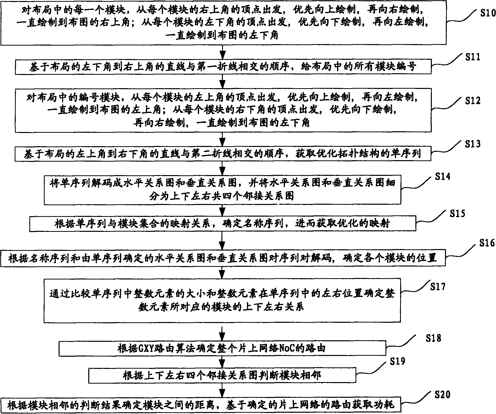
[0041] See figure 1 , the topology structure and mapping optimization method of the on-chip network in this embodiment includes the following steps:

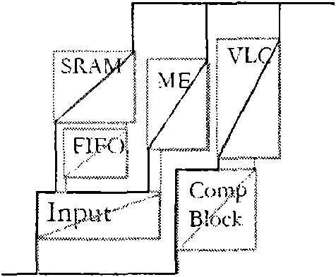
[0042]Step S10, for each module in the layout, start from the vertex in the upper right corner of each module, draw upward first, then draw to the right, and draw to the upper right corner of the layout; start from the vertex in the lower left corner of each module , draw downwards first, then draw to the left, and draw to the lower left corner of the layout;

[0043] Step S11, numbering all modules in the layout based on the order in which the straight line from the lower left corner to the upper right corner of the layout intersects with the first fold line;

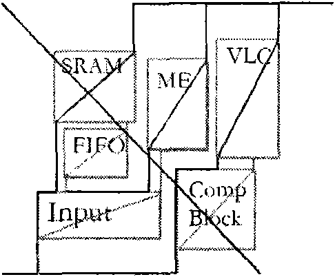
[0044] Step S12, for the numbered modules in the layout, start from the vertex in the upper left corner of each...


PUM


Abstract

The invention discloses a method for optimizing a topological structure and mapping of a network on chip (NoC), which comprises the following steps of: determining a single sequence (SS) for optimizing the topological structure through two drawing methods; and acquiring a name sequence for optimizing the mapping through a mapping relation between the single sequence (SS) and a module collection. So, the method can optimize a network structure and the mapping and reduce the power consumption. Besides, the method adopts a GXY routing algorithm to determine the routing of the entire network on chip (NoC), and performs optimization according to a simulated annealing algorithm to obtain a layout result that the power consumption is low and the area is small.

Description

technical field [0001] The invention relates to a general 2D topological structure based on layout planning technology, in particular to a network-on-chip (NoC, Network-on-Chip) topology and a mapping optimization method. Background technique [0002] With the continuous development of integrated circuit manufacturing technology, the number of transistors that can be accommodated on a single silicon chip is increasing, reaching billions of gates, which means that more and more IP cores can be integrated in a single chip. . The traditional bus structure cannot meet the communication requirements of dozens or even hundreds of IP cores. At this time, as a multi-processing system based on network communication implemented on a single chip, the network on chip can well solve the problems caused by the bus structure (see literature 1-4). It applies computer network technology to chip design, and obtains The result is better than that of the bus structure. [0003] However, in e...

Claims


Application Information

Patent Timeline
Patent Type & Authority Applications(China)
IPC IPC(8): H04L12/56H04L29/06G06F17/50H04L45/02
Inventor 徐宁郑飞
Owner WUHAN UNIV OF TECH
Why Eureka
Try Eureka