Light-emitting semiconductor connection structure and method thereof

A technology of light-emitting semiconductors and connection methods, which is applied to semiconductor devices, electrical components, circuits, etc., can solve the problems of unfavorable use of high-power light-emitting diodes, increased production costs, and low production efficiency, achieving strong bonding, increased production capacity, and reliable The effect of increasing

Inactive Publication Date: 2010-10-13
山东璨圆光电科技有限公司
View PDF0 Cites 0 Cited by
  • Summary
  • Abstract
  • Description
  • Claims
  • Application Information

AI Technical Summary

Problems solved by technology

However, if the metal flange uses solder, the melting point of the solder is too low, which is not conducive to the use of high-temperature processes and high-power light-emitting diodes (LEDs).
Furthermore, although the metal flanges can be prepared using gold (Au) bumps to improve the disadvantages of using solder, additional gold bumps are required, and in the method for preparing gold bumps, The number of gold bumps will determine the quality of its heat dissipation effect, and the preparation process of gold bumps required by high-power light-emitting diodes will increase its production cost and make its production efficiency low

Method used


Image

  • Light-emitting semiconductor connection structure and method thereof
  • Light-emitting semiconductor connection structure and method thereof
  • Light-emitting semiconductor connection structure and method thereof

Examples


Embodiment Construction

[0021] The preferred embodiments of the present invention will be further described in detail below with reference to the accompanying drawings. The ratio of certain dimensions relative to other parts is exaggerated to provide a clearer description and help those skilled in the art to understand the present invention.

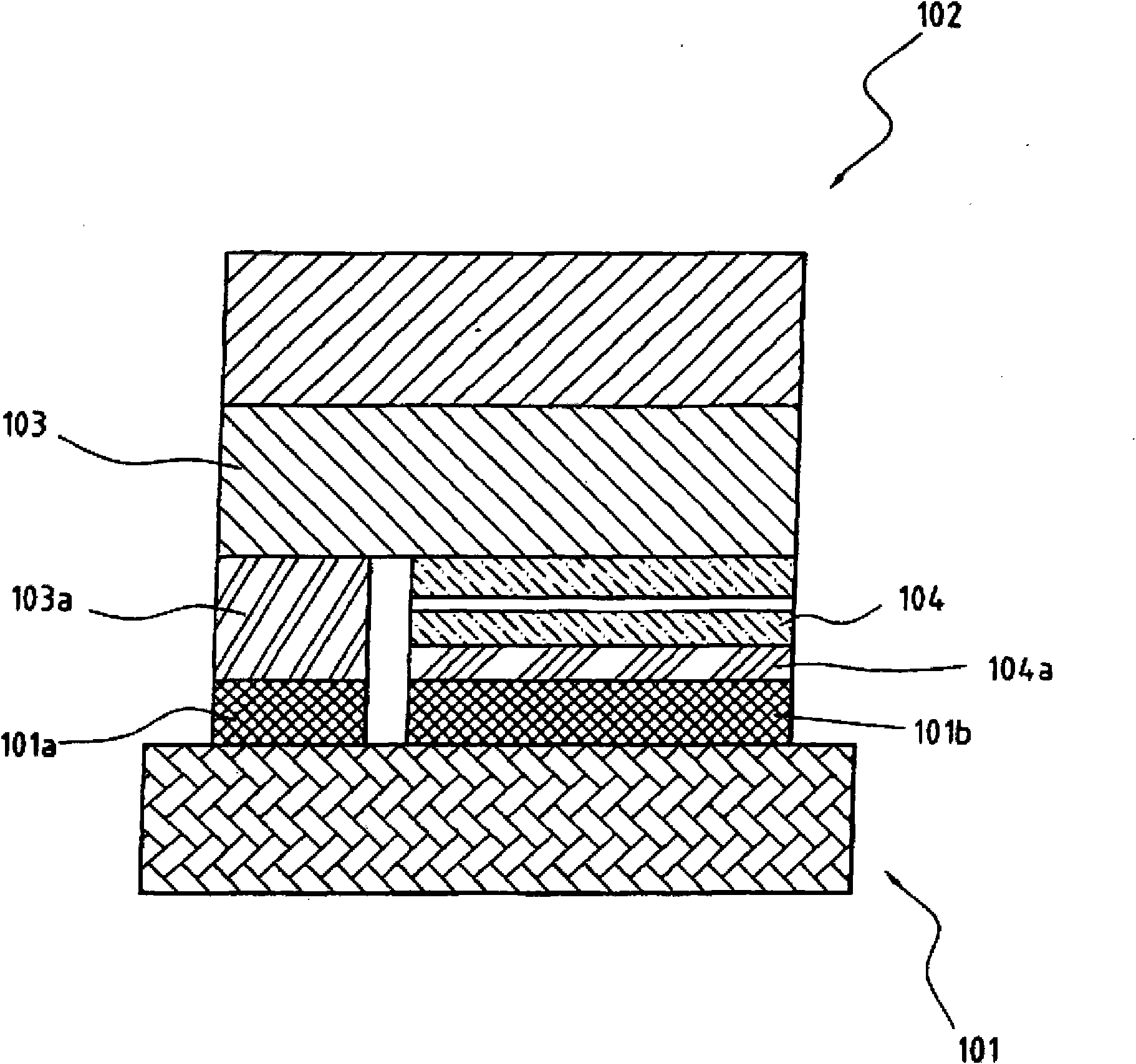
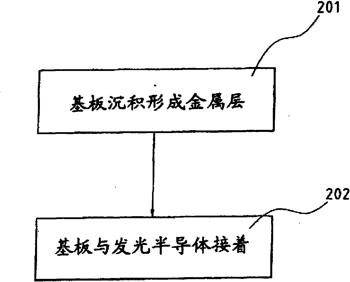
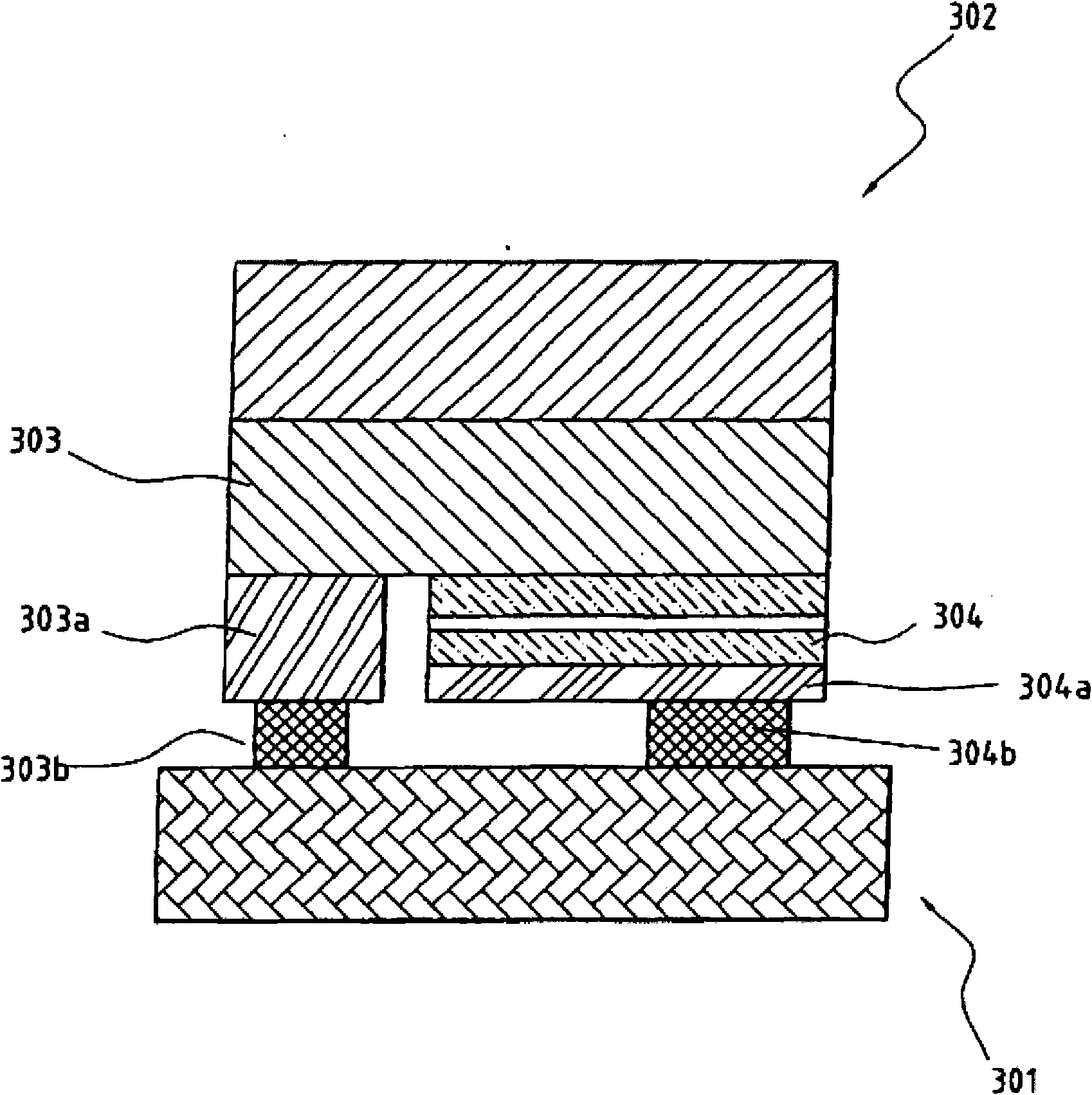
[0022] figure 1 Shown is a schematic cross-sectional view of a preferred embodiment of the light-emitting semiconductor connection structure and method thereof of the present invention; figure 2 shown as the invention figure 1 Preferred embodiment method flowchart.

[0023] refer to figure 1 As shown, the first embodiment of the light emitting semiconductor connection structure of the present invention is mainly a structure in which a light emitting semiconductor 102 is connected through a substrate 101 .

[0024] Wherein, the substrate 101 is a structure with electrical circuits, and at least a first metal layer 101a and a second metal layer 101b are f...


PUM


Abstract

The invention discloses a light-emitting semiconductor connection structure and a method thereof. the invention is mainly characterized by a structure that a base plate is connected with a light-emitting semiconductor, wherein the base plate is a structure provided with an electrical circuit, and an N type contact layer and a P type contact layer of the light-emitting semiconductor respectively form an ohmic-contact N electrode layer and an ohmic-contact P electrode layer; and the surface of the base plate forms a first metal layer and a second metal layer by a dip plating method or a deposition method, the first metal layer and the second metal layer are respectively electrically connected to electrical signal output/input nodes corresponding to the electrical circuit of the base plate, and the first metal layer and the second metal layer are respectively matched with the N electrode layer and the P electrode layer of the light-emitting semiconductor to enable the first metal layer and the second metal layer respectively correspond to the N electrode layer and the P electrode layer to realize mutual connection by ultrasonic welding, so that the light-emitting semiconductor is connected to the base plate and forms the electrical connection. The invention has the advantages of high engagement force, more uniform current distribution and better heat radiation, improves the reliability, and can lower the cost.

Description

technical field [0001] The present invention relates to a light-emitting semiconductor connection structure and method thereof, in particular to a light-emitting semiconductor connection structure and method for forming electrical connections on the substrate. Background technique [0002] In the conventional light-emitting semiconductor connection structure method, the light-emitting semiconductor is connected to an electrical control substrate through a general flip chip (flip chip) process. refer to image 3 The light-emitting semiconductor connection structure shown in the prior art is a structure in which a light-emitting semiconductor 302 is connected through a substrate 301 . Wherein, the substrate 301 is a structure with electrical circuits, and the light-emitting semiconductor 302 is a light-emitting diode component. Taking gallium nitride (GaN) as a light-emitting diode component, the light-emitting semiconductor 302 has an N-type contact layer 303 and a P-type co...

Claims


Application Information

Patent Timeline
Patent Type & Authority Applications(China)
IPC IPC(8): H01L33/00
Inventor 潘锡明简奉任
Owner 山东璨圆光电科技有限公司
Why Eureka
Try Eureka