Thermal interface material for packaging and radiating chip and preparation method thereof

A thermal interface material and chip packaging technology, applied in heat exchange materials, chemical instruments and methods, electrical components, etc., can solve the problems of poor contact and high thermal resistance, reduce thermal resistance of packaging, improve heat dissipation capacity and stability , Superior thermal contact effect

Inactive Publication Date: 2010-10-20
SUZHOU INST OF NANO TECH & NANO BIONICS CHINESE ACEDEMY OF SCI
View PDF4 Cites 19 Cited by
  • Summary
  • Abstract
  • Description
  • Claims
  • Application Information

AI Technical Summary

Problems solved by technology

[0006] In order to meet the needs of high-performance chip cooling technology and overcome the shortcomings of high thermal resistance and poor contact of existing thermal interface materials, the present invention provides a new type of thermal interface material for chip packaging and heat dissipation and its preparation method, which can be used in high-power chips Establish reliable thermal contact with the heat sink unit and provide sufficient thermal conductivity to improve the heat dissipation capability and reliable stability of high-power chips

Method used


Image

  • Thermal interface material for packaging and radiating chip and preparation method thereof
  • Thermal interface material for packaging and radiating chip and preparation method thereof

Examples


Embodiment Construction

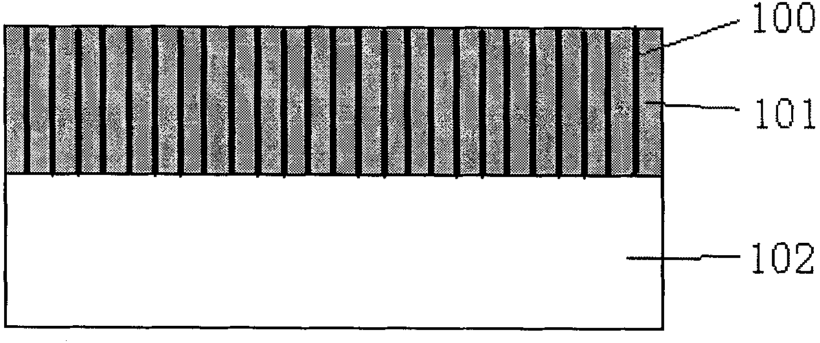
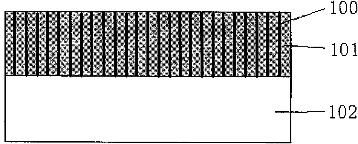
[0019] In order to meet the requirements of high-performance chip cooling technology and overcome the shortcomings of high thermal resistance and poor contact of existing thermal interface materials, the invention provides a thermal interface material used for chip packaging and having excellent heat dissipation. Such as figure 1 Shown is a schematic cross-sectional view of the thermal interface material, and it can be seen that the thermal interface material includes a carbon nanotube array formed by carbon nanotubes 100 on a substrate 102 and liquid metal 101 . in,

[0020] These carbon nanotubes 100 are all formed in a state perpendicular to the substrate 102 during preparation, and the diameter of the carbon nanotubes is about 2nm-100nm. The carbon nanotube array may be a single-wall carbon nanotube array, may be a double-wall carbon nanotube array, may also be a multi-wall carbon nanotube array or a single-wall, double-wall carbon nanotube array. The substrate 102 is an...


PUM

PropertyMeasurementUnit
thicknessaaaaaaaaaa
diameteraaaaaaaaaa
thicknessaaaaaaaaaa

Abstract

The invention discloses a thermal interface material for packaging and radiating a chip and a preparation method thereof. The thermal interface material comprises a carbon nano tube array on a substrate, and is characterized in that the thermal interface material contains liquid metal which is freely diffused and uniformly distributed in gaps of the carbon nano tube array. The invention uses the carbon nano tube having a high coefficient of heat conductivity to ensure that the thermal interface has a higher heat conductive property, uses the liquid alloy to promote the contact capability between the carbon nano tube and the heat sink and between the carbon nano tube and the chip so as to decrease the thermal resistance of the thermal interface and meet the radiating demand of high-performance chip. The preparation method thereof comprises the steps of: providing a carbon nano tube array vertically formed on the substrate, depositing a metal layer which is easily dissolved in liquid metal on the carbon nano tube, boosting to fully soak the carbon nano tube when the liquid metal is contacted with the carbon nano tube and filling the gaps of the carbon nano tube array.

Description

technical field [0001] The invention relates to a thermal interface material used for high-performance chip packaging and heat dissipation, in particular to a thermal interface material formed with a carbon nanotube array as a basic component and a preparation method thereof. Background technique [0002] According to the famous "Moore's Law" calculation: the number of transistors on a chip doubles every 18 months, then by 2010, the number of transistors on a chip will exceed 1 billion. High integration is beneficial to the upgrade of computer performance, but the problems of chip energy consumption and heat dissipation are also highlighted. In fact, in addition to computer chips, for a large number of power electronic devices, optoelectronic devices, and micro / nano electromechanical systems that have developed rapidly in recent years, there are similar extensive and urgent heat dissipation and cooling needs, and even higher requirements in some cases. . For example, the h...

Claims


Application Information

Patent Timeline
Patent Type & Authority Applications(China)
IPC IPC(8): C09K5/08H01L23/373
Inventor 吴东岷李加东
Owner SUZHOU INST OF NANO TECH & NANO BIONICS CHINESE ACEDEMY OF SCI
Why Eureka
Try Eureka