Unlock instant, AI-driven research and patent intelligence for your innovation.

Detector

A detection device and slide rail technology, applied in the direction of measuring devices, measuring electricity, measuring electrical variables, etc., can solve problems such as bulky, complicated adjustment methods of the lead screw 131, deformation of the lead screw 131, etc.

Inactive Publication Date: 2012-05-23
MPI CORP
View PDF1 Cites 0 Cited by
  • Summary
  • Abstract
  • Description
  • Claims
  • Application Information

AI Technical Summary

Problems solved by technology

[0004] Ideally, when the carrier table 13 drives the wafer 15 up, the plurality of probes 121 should be able to contact with the contact pads (not shown) on the corresponding wafer 15 simultaneously, so as to carry out the process on the wafer 15. For the test, in order to adjust the parallelism between the carrying table 13 and the probe 121, the general industry is to set the carrying table 13 on a plurality of lead screws 131, and then wrap the carrying table 13 and the lead screws 131 with castings as In one piece, in order to support the carrying platform 13 stably, at least four lead screws 131 must be provided, which is bulky and takes up space, and the adjustment method of the lead screws 131 is complicated, difficult and time-consuming. In addition, the lead screws 131 It is usually driven by a motor and a belt, and the belt has a flexibility problem. When the belt bears a high load, it will affect the accuracy of the actual height adjustment
Furthermore, if the supporting strength of the lead screw 131 itself is insufficient, the lead screw 131 will be deformed, which will affect the flatness of the loading platform 13
Finally, the reliability of the lead screw 131 is not good, and it is easy to cause the accuracy of the flatness of the loading platform 13 to decrease.
[0005] As far as patents are concerned, it is known that Taiwan Province of China Invention Patent Application No. 91133971 "In the semiconductor automated wafer test, the device and method for ensuring the parallelism of the probe card to the wafer, the probe card measurement system, and the probe card "Manufacturing", which discloses a technical means of using an optical target to detect the parallelism between the probe and the wafer, but the cost of the method and system is extremely high

Method used


Image

  • Detector
  • Detector
  • Detector

Examples


Embodiment Construction

[0014] The technical means and functions used by the present invention to achieve the purpose will be described below with reference to the accompanying drawings, and the embodiments listed in the following figures are only for auxiliary explanation, so as to facilitate your examiner's understanding, but the technical means in this case are not limited to the above-mentioned List the schema.

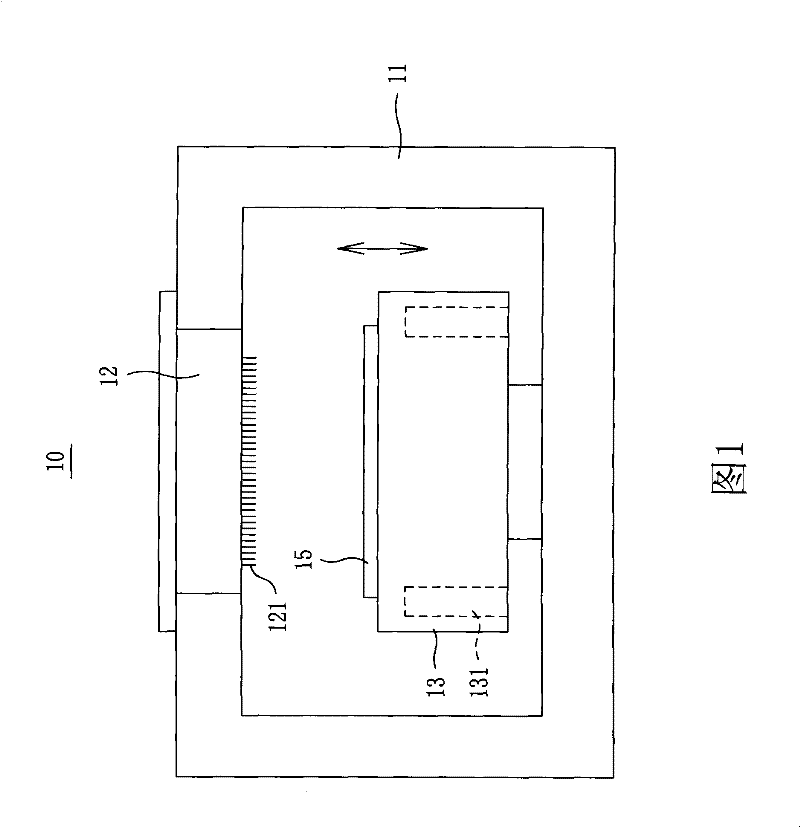
[0015] see Figure 2 to Figure 4 As shown, the structure of the embodiment of the detection device 20 proposed by the present invention includes a base 21 , a wedge 22 , a limiting structure 23 , a carrying platform 24 and a slide rail set 25 .

[0016] A wedge block 22 is provided on the base 21 for horizontal displacement of the wedge block 22 on the base 21 . The limiting structure 23 is arranged on one side of the base 21 and fixed on the base 21 . The bearing platform 24 includes two parts: a bearing base 241 and a bearing base 242 , the bearing base 241 is fixedly disposed on the...


PUM


Abstract

The invention discloses a detector, which mainly comprises a base, a wedge-shaped block arranged on the base, a limiting mechanism arranged on one side of the base, a bearing table having a bearing support which is arranged on the limiting mechanism, a slide track set arranged between the bearing support and the wedge-shaped block and a driver, wherein the limiting mechanism is arranged for limiting the vertical displacement of the bearing support, and the driver is arranged for driving the horizontal displacement of the wedge-shaped block and driving the vertical displacement of the bearing support via the slide track set. Due to the designs of the bearing support and the wedge-shaped block and the collocation of the slide track set, the loading capacity of the bearing table is increased, deformation is avoided, and the adjustment on the parallelism of the bearing table is facilitated.

Description

technical field [0001] The invention relates to a detection device, in particular to a detection device for semiconductors and light-emitting diodes. Background technique [0002] Manufacturing of semiconductors and light-emitting diodes can be divided into 1C Design, Wafer Fabrication, Wafer Probe, and Packaging. Wafers must be tested multiple times. , such as circuit conduction state, aging, high temperature and other tests can ensure its quality. Wherein, the detecting device is used for detecting the wafer. [0003] see figure 1 A schematic structural view of an existing detection device is shown, the detection device 10 has a support frame 11, a probe card 12 is arranged on the top of the support frame 11, and a plurality of probe cards are arranged on the bottom of the probe card 12. Needle 121, the wafer detection device 10 is provided with a carrying platform 13, and then the wafer 15 is placed on the carrying platform 13, and the carrying platform 13 can be moved...

Claims


Application Information

Patent Timeline
Patent Type & Authority Patents(China)
IPC IPC(8): H01L21/68G01R31/26G01R1/02
Inventor 杨天德
Owner MPI CORP