
Plasma etching method for etching organic matter layer

An organic and plasma technology, applied in electrical components, semiconductor/solid-state device manufacturing, circuits, etc., can solve the problems of uneven etching morphology in the middle area and edge area, bow shape in the edge area of ​​the substrate, etc., and achieve uniform etching effect. Effect

Active Publication Date: 2012-05-30
ADVANCED MICRO FAB EQUIP INC CHINA
View PDF0 Cites 0 Cited by
  • Summary
  • Abstract
  • Description
  • Claims
  • Application Information

AI Technical Summary

Problems solved by technology

However, in the actual etching process, the researchers found that when such a gas composition is mixed and then fed into the reaction chamber for etching, the middle area of ​​the substrate will obtain a better etching effect, while the edge area of ​​the substrate will appear severely bowed. )Happening
Moreover, this situation is difficult to improve, because the oxygen-containing etching gas and the reaction gas that can improve the bow shape have been mixed before entering the reaction area, so the gas ratio of the two is relatively relative to the middle area and the middle area of ​​the substrate. The edge area is the same, and it is fixed and cannot be adjusted, so even adjusting the ratio of the mixed gas intake rate between the middle and the edge still cannot effectively improve this situation, and eventually the middle area and edge area of ​​the substrate appear uneven etching appearance

Method used


Image

  • Plasma etching method for etching organic matter layer
  • Plasma etching method for etching organic matter layer
  • Plasma etching method for etching organic matter layer

Examples


Embodiment Construction

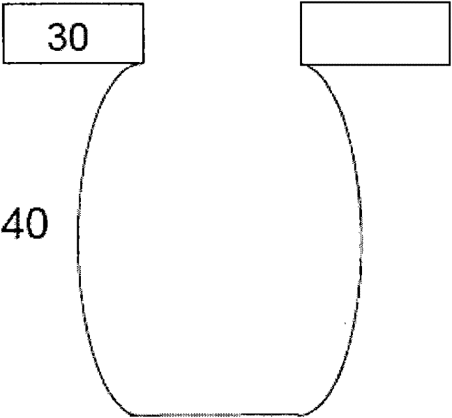
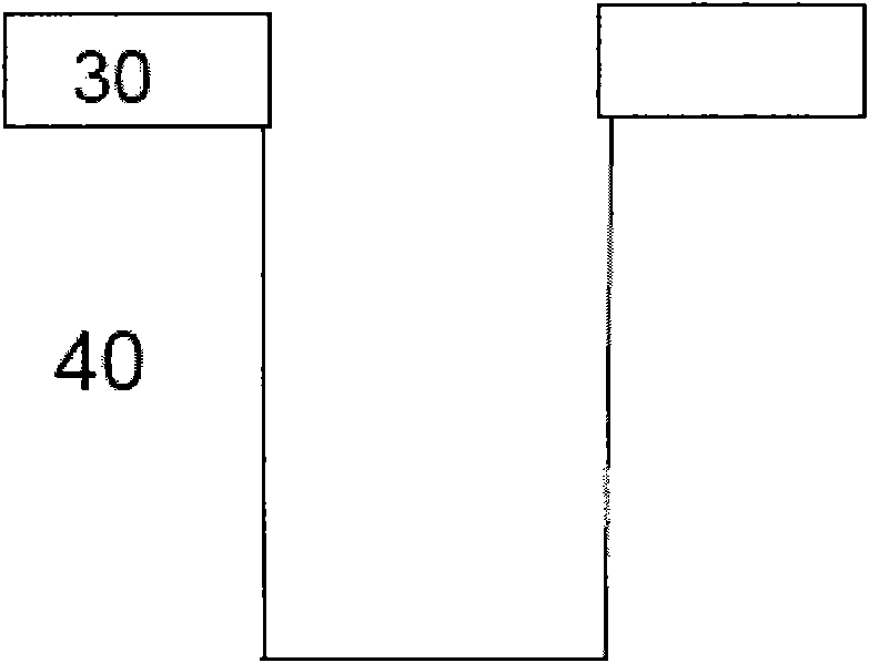
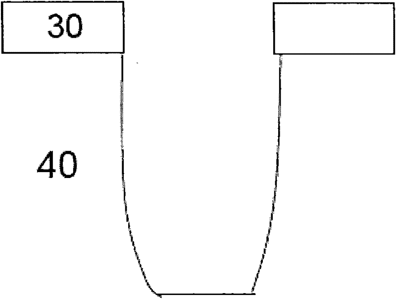
[0018] In the prior art, a mixed etching gas and a sidewall protection gas are used for etching, and the etching gas is one of oxygen-containing gases such as O2, CO2, and CO or a mixed gas. The sidewall protection gas may be a sulfur-containing gas (such as COS), which can form a solid protective layer on the sidewall formed by etching the carbon-containing layer, preventing the sidewall from being etched and forming a bow. The sidewall shielding gas can also be a polymer forming gas (such as hydrocarbon or fluorocarbon) to form a thick enough polymer on the etched sidewall. Due to the limitation of the hardware structure of the etching reaction chamber, there will inevitably be uneven plasma density between the central area and the edge area of ​​the substrate (high in the middle and low at the edge), and the edge area will also be affected by the exhaust device to reduce the gas concentration. These factors all lead to different groove profiles formed by etching in the cent...


PUM


Abstract

The invention relates to a plasma etching method for etching an organic matter layer, aiming to solve the problem that when an organic matter layer is etched, the central area and the marginal area of a substrate has non-uniform etching effects. In the etching method, a gas distributing device is utilized to supply etching gas for the central area of the substrate, and supply side wall protectivegas for the marginal area of the substrate, wherein the etching gas and the side wall protective gas are mutually isolated before entering a reaction area above the substrate in a reaction cavity. When introduced into the reaction cavity from the gas distributing device, the etching gas and the side wall protective gas are gradually dispersed and mixed, and finally, reaction gas containing the etching gas and the side wall protective gas in different mixing proportions is obtained on the surface of the substrate. The different mixing proportions ensure that the central area and the marginal area of the substrate can counteract etching effect difference caused by other factors, and finally, the central area and the marginal area have uniform etching effect.

Description

technical field [0001] The invention relates to the field of manufacturing semiconductor devices, in particular to a plasma etching method for an organic layer. Background technique [0002] The etching process refers to the process of removing unnecessary parts in the substrate or in the film layer on the surface of the substrate by using chemical solution or corrosive gas or plasma in the process of manufacturing semiconductor devices. Generally, the etching method mainly using chemical solution is wet etching, and the etching method using corrosive gas or plasma is dry etching. At present, dry etching, which can make circuit patterns finer, is more and more widely used. [0003] In wet etching, the chemical reaction of strong acid is used for isotropic etching, even the part covered by the mask can be etched. In contrast, dry etching uses reactive ion etching, in which etching is performed with a corrosive chemical gas, such as a halogen in a plasma, and plasma ions. T...

Claims


Application Information

Patent Timeline
IPC IPC(8): H01L21/311
Inventor 高山星一陶铮倪图强
Owner ADVANCED MICRO FAB EQUIP INC CHINA
Learn More