
Copper wiring plasma etching method

A technology of plasma and plasma reaction, which is applied in semiconductor/solid-state device manufacturing, electrical components, circuits, etc., can solve the problem that the consistency of etching processing cannot be guaranteed, and achieve the effect of uniform etching effect

Active Publication Date: 2012-04-04
ADVANCED MICRO FAB EQUIP INC CHINA
View PDF4 Cites 0 Cited by
  • Summary
  • Abstract
  • Description
  • Claims
  • Application Information

AI Technical Summary

Problems solved by technology

The consistency of etching processing cannot be guaranteed

Method used


Image

  • Copper wiring plasma etching method
  • Copper wiring plasma etching method
  • Copper wiring plasma etching method

Examples


Embodiment Construction

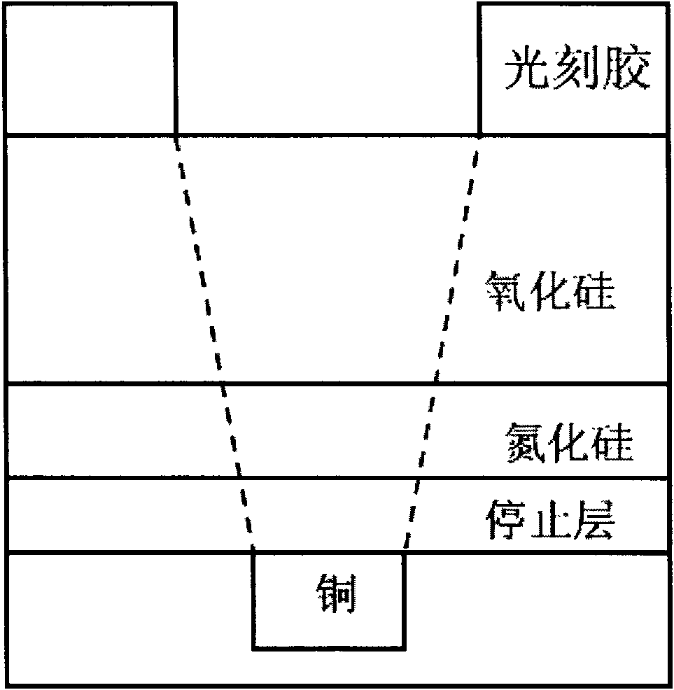
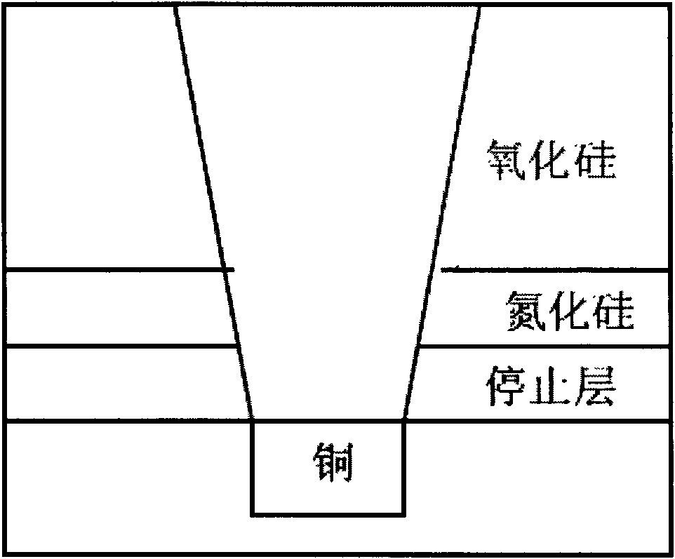
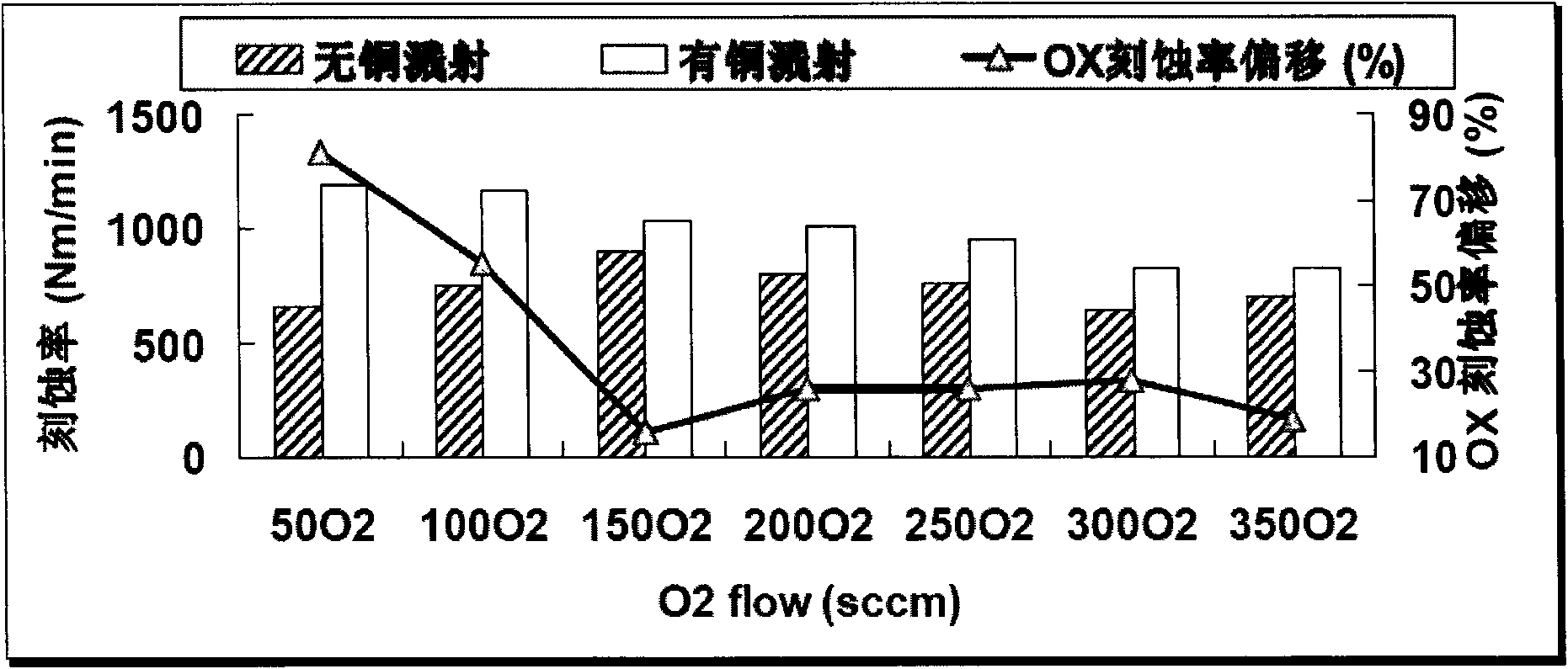
[0014] In the prior art, the etch rate significantly shifts under the condition of copper sputtering. The present invention suppresses the influence of sputtered copper on the production process by optimizing the etching process. The inventor found through research that when sputtering copper in an atmosphere with a large amount of oxidizing gas, the catalytic effect of copper on the etching reaction is not obvious, so that the deviation of the etching reaction rate caused by copper exposure in the reaction chamber can be suppressed , the recovery speed of the state of the reaction chamber is also greatly accelerated.

[0015] In the present invention, in addition to feeding etching gases such as fluorocarbons, a large amount of oxidizing gas is also fed during the etching process, and the oxidizing gas can be O2, CO2, N2O, O3 or other gases with oxidation functions. Compared with the amount of oxidizing gas in the prior art which is only 0-100 sccm, in order to achieve the pu...


PUM


Abstract

The invention discloses a copper wiring plasma etching method, which resolves the problem of etching speed deviation caused by copper atoms sputtered and exposed to a reaction cavity during etching. During etching of a silicon-contained insulating layer until exposure of a lower copper layer, original etching gas flow can be maintained while oxygen-contained gas flow is increased during etching by the copper wiring plasma etching method. After mixing ratio of oxygen and etching gas is increased, the problem of etching speed deviation caused by copper exposed into the reaction cavity is resolved, and long-term, uniform and stable processing effects can be obtained more easily.

Description

technical field [0001] The invention relates to the field of manufacturing semiconductor devices, in particular to a plasma etching method for copper process. Background technique [0002] The etching process refers to the process of removing unnecessary parts in the wafer or in the film layer on the surface of the wafer by using chemical solution or corrosive gas or plasma in the process of manufacturing semiconductor devices. Generally, the etching method mainly using chemical solution is wet etching, and the etching method using corrosive gas or plasma is dry etching. At present, dry etching, which can make circuit patterns finer, is more and more widely used. [0003] In wet etching, the chemical reaction of strong acid is used for isotropic etching, even the part covered by the mask can be etched. In contrast, dry etching uses reactive ion etching, in which etching is performed with a corrosive chemical gas, such as a halogen in a plasma, and plasma ions. Therefore, ...

Claims


Application Information

Patent Timeline
Patent Type & Authority Applications(China)
IPC IPC(8): H01L21/311
Inventor 王兆祥刘志强黄智林
Owner ADVANCED MICRO FAB EQUIP INC CHINA
Learn More