NPN transistor and fabricating method thereof

A technology of transistors and manufacturing methods, applied in the direction of transistors, semiconductor/solid-state device manufacturing, semiconductor devices, etc., can solve problems such as lateral and transient diffusion effects, and achieve the effects of reducing lateral and transient diffusion and reducing series resistance

Inactive Publication Date: 2010-10-20
SHANGHAI HUAHONG GRACE SEMICON MFG CORP
View PDF5 Cites 2 Cited by
  • Summary
  • Abstract
  • Description
  • Claims
  • Application Information

AI Technical Summary

Problems solved by technology

[0008] The NPN transistor formed by the prior art reduces the series resistance due to one-time high-dose and high-energy ion implantation at the emitter 110 and the base 106, but it will cause negative effects of lateral and transient diffusion

Method used


Image

  • NPN transistor and fabricating method thereof
  • NPN transistor and fabricating method thereof
  • NPN transistor and fabricating method thereof

Examples


Embodiment Construction

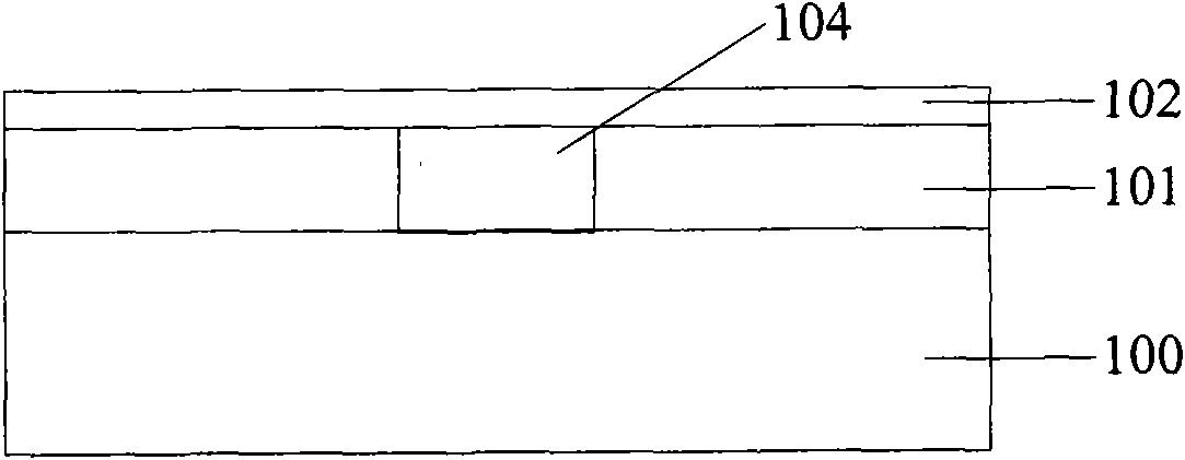
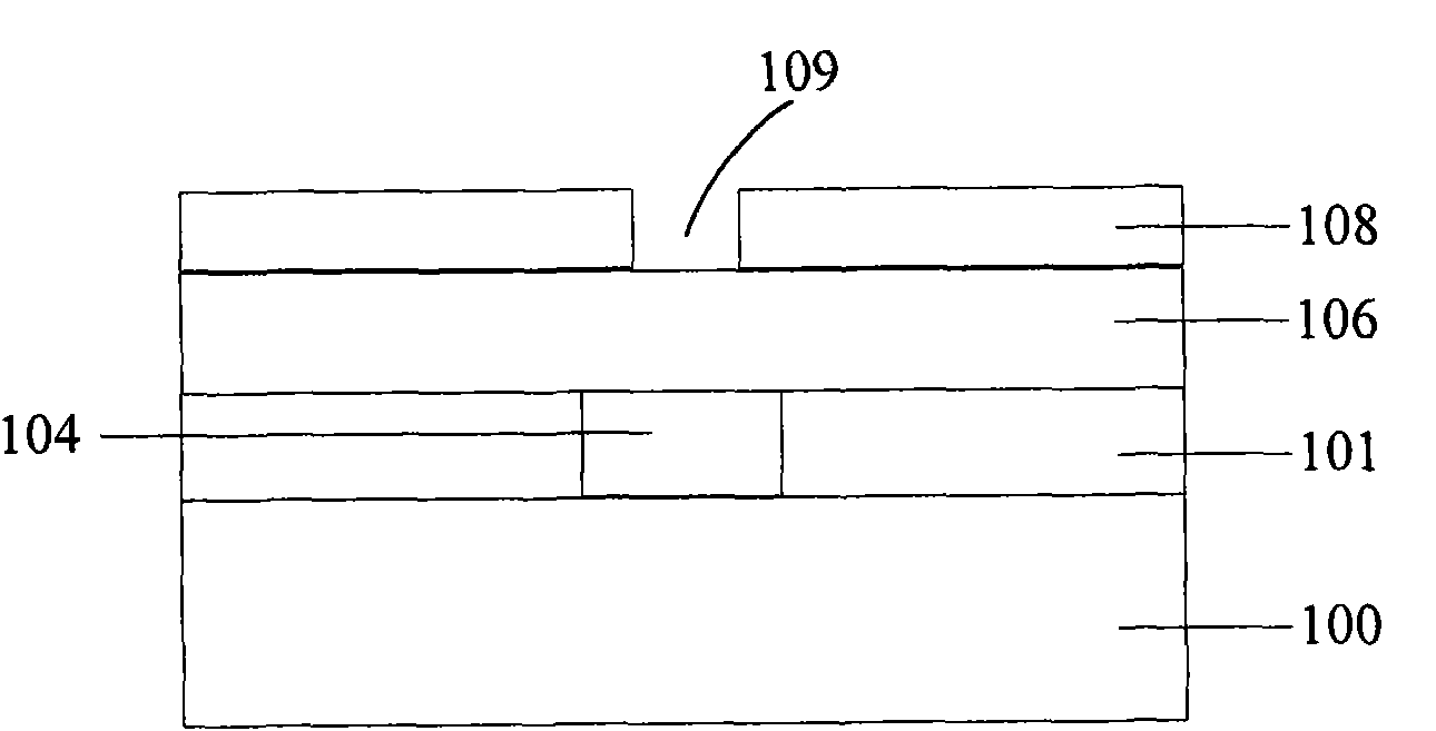
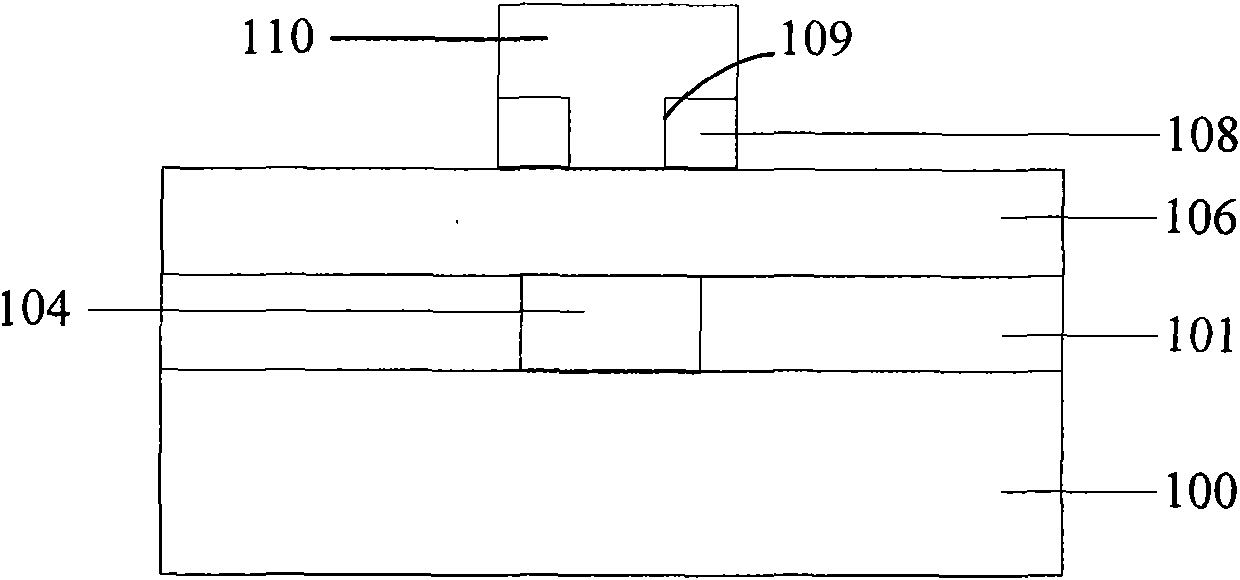
[0016] The specific implementation flow process of forming NPN transistor in the present invention is as follows Figure 5 As shown, step S1 is performed to provide a semiconductor substrate, and an N-type buried layer region is formed in the semiconductor substrate; step S2 is performed to form a first oxide layer on the N-type buried layer region, and the N-type buried layer region Implanting ions to form a collector; performing step S3, after removing the first oxide layer, forming a P-type epitaxial layer on the N-type buried layer region as a base; performing step S4, forming a contact hole on the P-type epitaxial layer After the second oxide layer, a polysilicon layer that fills the contact hole and covers the second oxide layer is formed; step S5 is performed to etch the polysilicon layer and the second oxide layer to expose the P-type epitaxial layer, and the etched polysilicon layer is used as Emitter; perform step S6, form shallowly doped metal contacts in the base o...


PUM


Abstract

The invention provides an NPN transistor and a fabricating method thereof, wherein the NPN transistor comprises a semiconductor substrate, an N-type buried layer region positioned in the semiconductor substrate, a collector electrode positioned in the N-type buried layer region, base electrodes positioned on the N-type buried layer region and the collector electrode, a second oxidization layer positioned on the surface of the base electrodes, an emitting electrode, shallow-doped metal contacts positioned in the base electrodes at two sides of the emitting electrode, side walls positioned at two sides of the emitting electrode and the second oxidization layer and deep-doped regions positioned in the emitting electrode and the base electrodes at two sides of the side walls, wherein the second oxidization layer is internally provided with a contact hole penetrating the thickness of the second oxidization layer; the emitting electrode is filled in the contact hole and cover the surface of the second oxidization layer around the contact hole; and the deep-doped regions are deeper than shallow-doped regions in the base electrodes. The invention can greatly reduce the series resistance, and can lower the influence of side and transient diffusion.

Description

technical field [0001] The invention relates to the field of semiconductor device manufacturing, in particular to an NPN transistor and a manufacturing method thereof. Background technique [0002] Bipolar transistors are one of the device structures that constitute modern large-scale integrated circuits. Bipolar transistors have the advantages of fast operation speed, large output current per unit chip area, and small changes in conduction voltage, which are suitable for making analog circuits. [0003] With the continuous development of semiconductor technology, the performance requirements of devices are getting higher and higher, and the performance requirements of bipolar transistors (such as NPN transistors) are also correspondingly increased. [0004] The existing process for forming NPN transistors is as follows: figure 1 As shown, a semiconductor substrate 100 is provided, and the material of the semiconductor substrate 100 can be silicon or silicon germanium, etc....

Claims


Application Information

Patent Timeline
Patent Type & Authority Applications(China)
IPC IPC(8): H01L21/331H01L21/265H01L29/73H01L29/36
Inventor 孙涛陈乐乐曼纽拉·奈耶尔
Owner SHANGHAI HUAHONG GRACE SEMICON MFG CORP
Why Eureka
Try Eureka