
Interlock of read column select and read databus precharge control signals

A technology for reading data and data bus, which is applied in timing control of column selection and precharge signal. field, which can solve problems such as slow device execution

Inactive Publication Date: 2010-10-27
CONVERSANT INTPROP MANAGEMENT INC
View PDF5 Cites 8 Cited by
  • Summary
  • Abstract
  • Description
  • Claims
  • Application Information

AI Technical Summary

Problems solved by technology

In order to account for the propagation delay of the signal to ensure data integrity, more timing margin can be provided, but this will cause the device to perform slower

Method used


Image

  • Interlock of read column select and read databus precharge control signals
  • Interlock of read column select and read databus precharge control signals
  • Interlock of read column select and read databus precharge control signals

Examples


Embodiment Construction

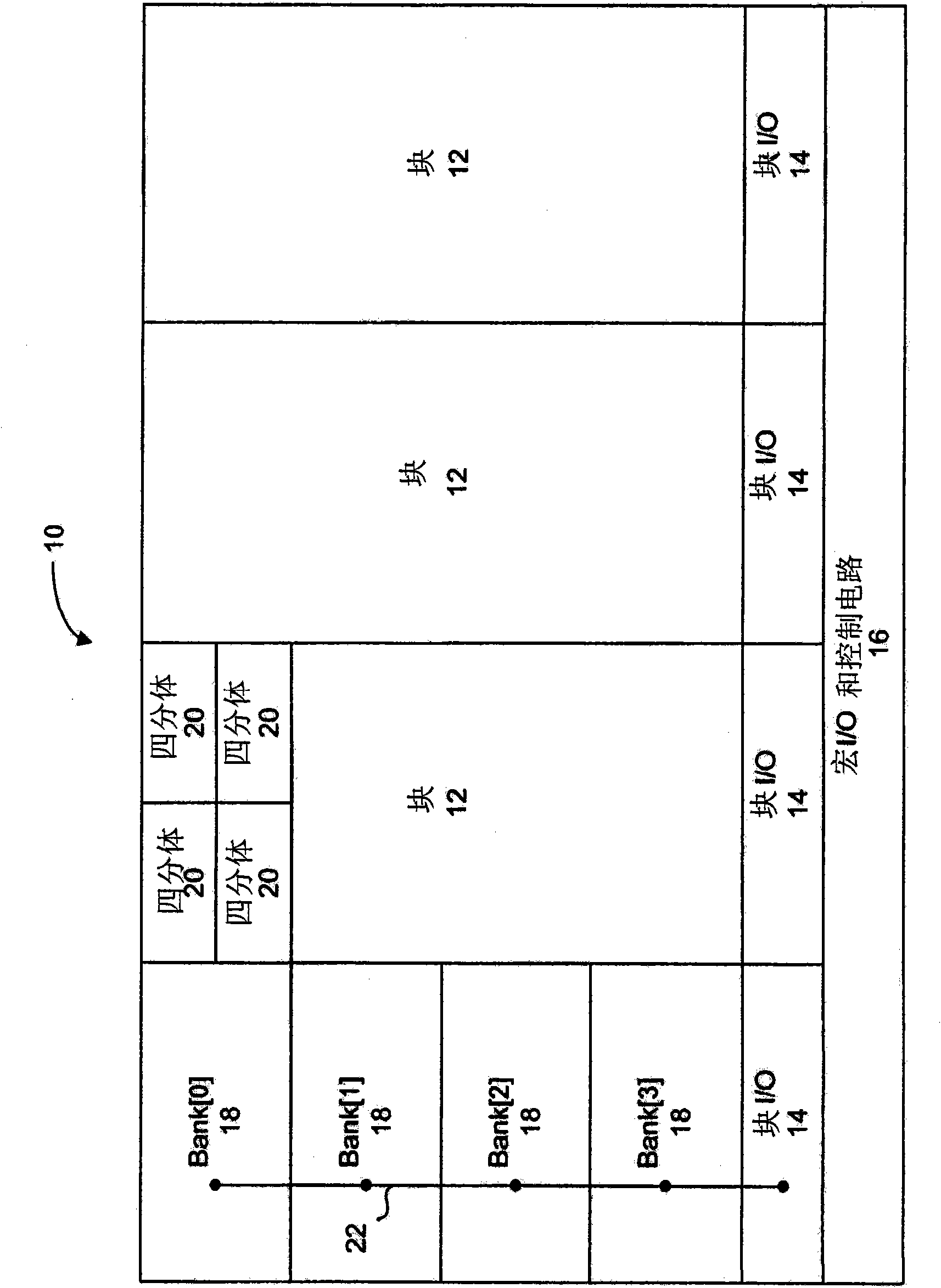
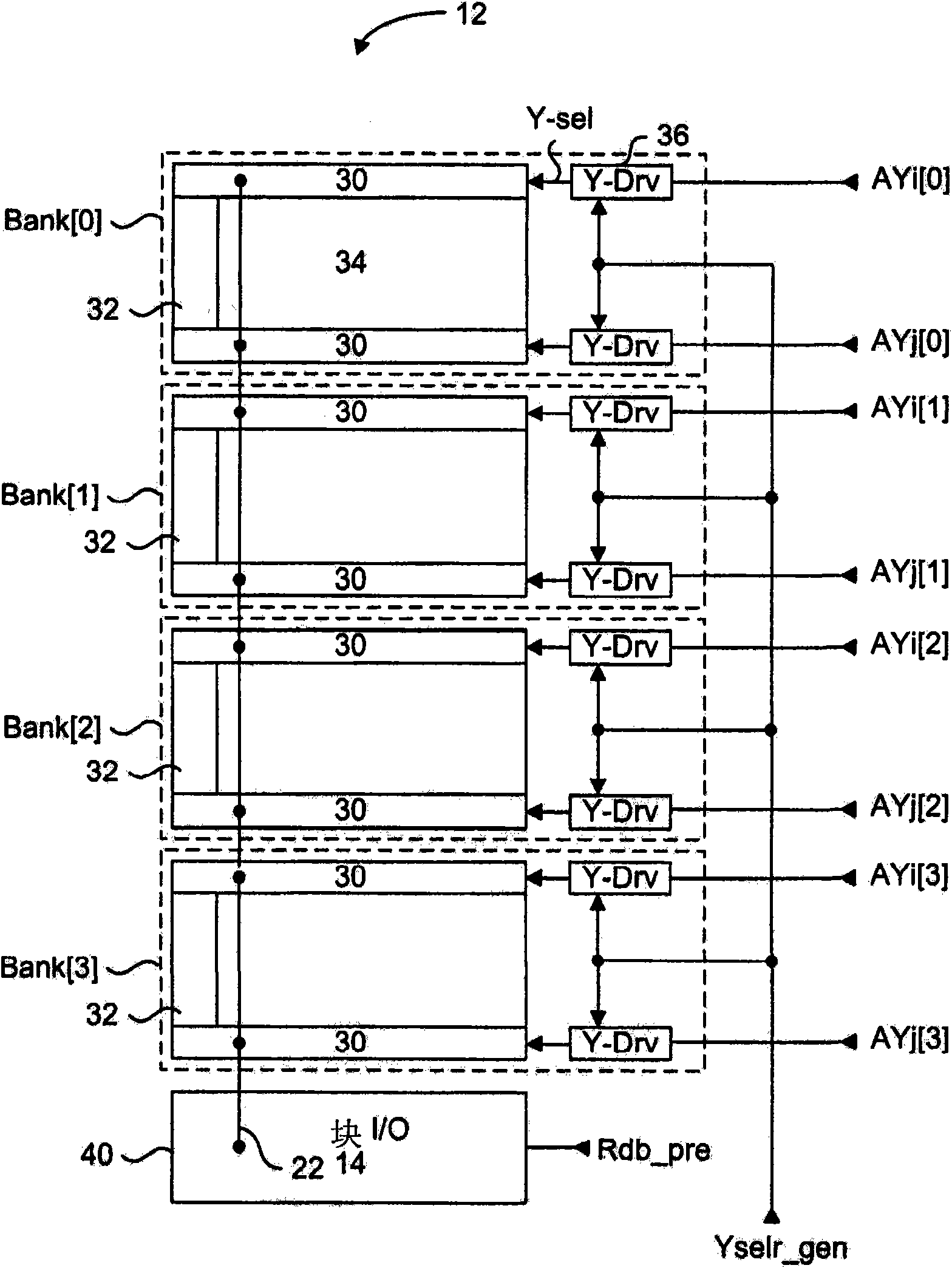
[0040] The invention discloses a column selection and precharge signal interlock scheme for DRAM memory. The signal interlock system includes a column sense enable circuit associated with each bank of the DRAM memory for generating a column select signal for coupling data to a common sense data bus and for generating a column select signal for disabling the sense data Read data bus precharge disable signal for bus precharge device. Each column read enable circuit includes a pulse generator circuit having an adjustable element for generating at least one column select signal pulse and a read data bus precharge disable pulse during a read operation. The circuitry in the pulse generator circuit ensures that the column select pulse is always embedded with the read data bus precharge disable pulse. Thus, there is no overlap between active column select means and active read data bus precharge means.

[0041] In fact, the column select signal pulses and precharge disable signal puls...


PUM


Abstract

A column select and databus precharge signal interlock scheme for a DRAM memory. The signal interlock system includes column read enable circuits associated with each bank of a DRAM memory for generating column select signals for coupling data to a common read databus, and a read databus precharge disable signal for disabling read databus precharge devices. Each column read enable circuit includes pulse generator circuits with tunable components for generating at least one column select signal pulse and the read databus precharge disable pulse in a read operation. The pulse generator circuits ensure that the column select pulse is always nested with respect to the read databus precharge disable pulse. Therefore, there is no overlap between active column select devices and active read databus precharge devices.

Description

technical field [0001] The present invention relates generally to semiconductor memories. More specifically, the present invention relates to column selection and precharge signal timing control. Background technique [0002] DRAM memories are widely used in computer systems due to their high density and high performance relative to other available memories. DRAM memory can be used in other applications such as hard disk drive cache to quickly access large amounts of data storage. Although the performance of SRAM is comparable, SRAM memory cells are relatively large, resulting in a low storage density per cell area of ​​the chip. On the other hand, flash memory has better storage density than DRAM, but read and write (program) performance is relatively poor. Thus, DRAM offers the best balance between storage density and performance. [0003] Those of ordinary skill in the art should be very familiar with DRAM architecture. A DRAM memory array includes rows of word lines...

Claims


Application Information

Patent Timeline
Patent Type & Authority Applications(China)
IPC IPC(8): G11C8/08G11C11/401G11C7/10G11C7/18G11C8/18
CPCG11C11/4096G11C8/12G11C11/408G11C11/4087
Inventor V·L·莱恩斯
Owner CONVERSANT INTPROP MANAGEMENT INC
Learn More