Chemical mechanical polishing device, polishing method and system for wafer

A technology of chemical machinery and grinding method, which is applied in the direction of electrical components, grinding devices, grinding machine tools, etc., can solve the problems of inconvenience, general products and methods without suitable structures and methods, etc., to reduce the use, reduce the chemical reaction time, reduce the The effect of dishing or erosion

Active Publication Date: 2010-11-10
TAIWAN SEMICON MFG CO LTD
View PDF0 Cites 16 Cited by
  • Summary
  • Abstract
  • Description
  • Claims
  • Application Information

AI Technical Summary

Problems solved by technology

[0009] This shows that the above-mentioned existing chemical mechanical polishing process obviously still has inconvenience and defects in method and use, and needs to be further improved urgently
In order to solve the above-mentioned problems, the relevant manufacturers have trie...

Method used


Image

  • Chemical mechanical polishing device, polishing method and system for wafer
  • Chemical mechanical polishing device, polishing method and system for wafer
  • Chemical mechanical polishing device, polishing method and system for wafer

Examples


Embodiment Construction

[0076] In order to further illustrate the technical means and effects that the present invention adopts for reaching the intended invention purpose, below in conjunction with the accompanying drawings and preferred embodiments, the chemical mechanical polishing element, the polishing method of the wafer and the wafer polishing system proposed according to the present invention will be described. ) Its specific implementation, structure, method, step, feature and effect thereof are described in detail as follows.

[0077] The aforementioned and other technical contents, features and effects of the present invention will be clearly presented in the following detailed description of preferred embodiments with reference to the drawings. For convenience of description, in the following embodiments, the same elements are denoted by the same numbers.

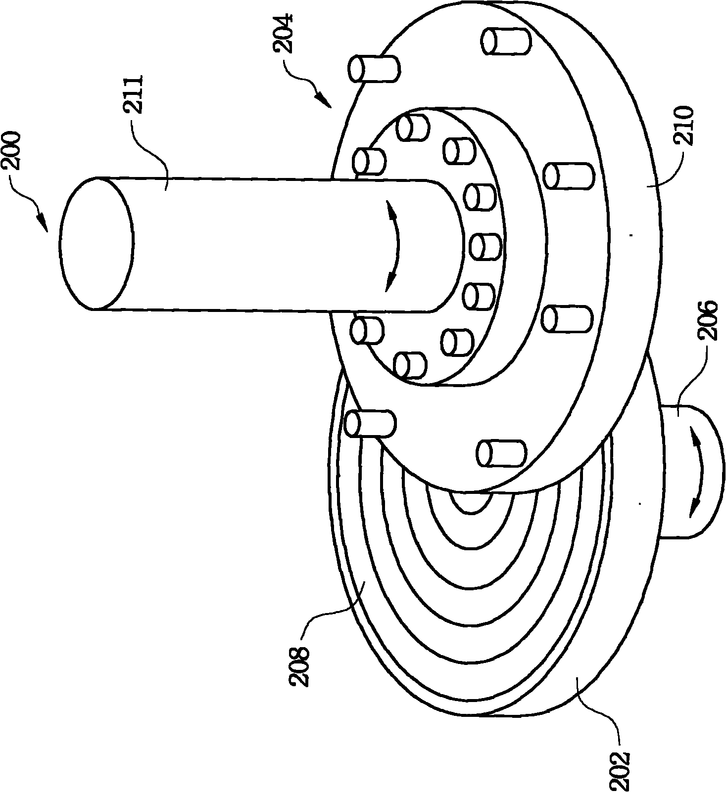
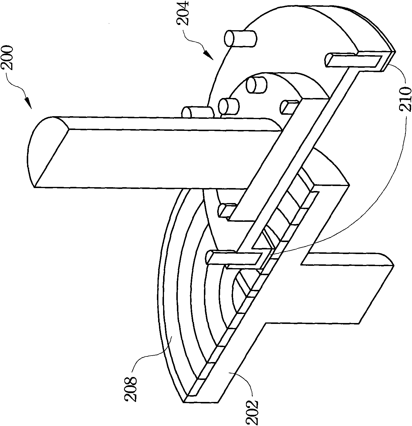
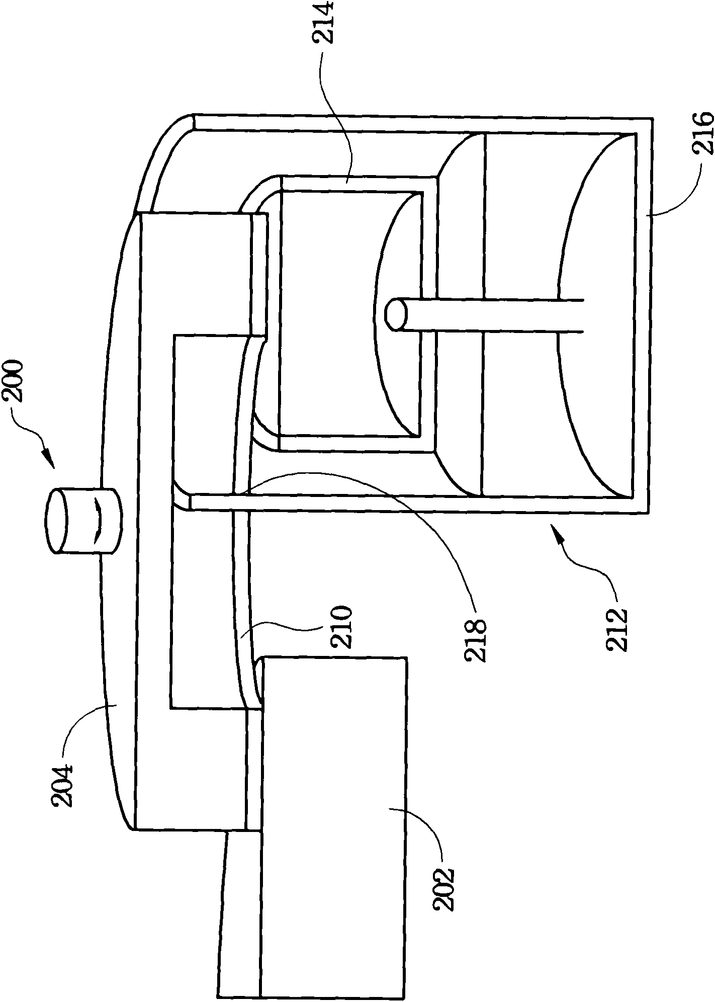
[0078] The present invention relates to a semiconductor substrate polishing apparatus, and in many embodiments, more particularly to ...


PUM


Abstract

The present invention relates to a chemical mechanical polishing device, and a method and a system of polishing a wafer, wherein the chemical mechanical polishing device for processing the wafer includes a plate for supporting the wafer to be processed in a face-up orientation; a polishing head opposing the plate, wherein the polishing head includes a rotatable polishing pad operable to contact the wafer while the polishing pad is rotating; and a slurry coating system providing a slurry to the polishing pad for polishing the wafer. By means of the invention, it is possible to perform a chemical mechanical polishing process to the face-up wafer; thereby, it is possible to reduce bending degree of the wafer and generate a better whole plainness degree so as to save a process window time of a scanner, it is also possible to reduce chemical reaction time so as to reduce dish-shaped appearance generation or corrosion in micro-shadow treatment. Furthermore, the wafer is faced upwards, such that it is possible to monitor the surface of the in-site wafer simply to implement accurate polishing control so as to be more practical.

Description

technical field [0001] The present invention relates to a semiconductor substrate grinding equipment, in particular to a chemical mechanical polishing (CMP) equipment, a chemical mechanical grinding element capable of performing a face-up wafer chemical mechanical grinding process, a wafer grinding method and a wafer grinding system. Background technique [0002] The semiconductor integrated circuit industry has experienced rapid growth. Technological advances in integrated circuit materials and design have produced generations, each generation having smaller and more complex circuits than the previous generation. However, these advances have increased the complexity of processing and manufacturing integrated circuits, and to realize these advances, similar developments in integrated circuit processing and manufacturing systems are required. [0003] During the development of integrated circuits, functional density (ie, the number of interconnected elements per wafer area)...

Claims


Application Information

Patent Timeline
IPC IPC(8): B24B37/04B24B57/02B24B53/12B24B55/00H01L21/00H01L21/306
CPCB24B57/02H01L21/02052B24B53/017B24B37/107
Inventor 林俞良黄见翎汪青蓉余振华
Owner TAIWAN SEMICON MFG CO LTD
Why Eureka
Try Eureka