Method and device for measuring three-dimensional topography of nano structure

A technology of nanostructures and measurement methods, applied in the direction of measuring devices, optical devices, instruments, etc., can solve the problems of inability to obtain three-dimensional shape information of nanostructures, and achieve the effect of promoting extended applications, wide application prospects, and high spectral sensitivity

Active Publication Date: 2010-11-10
WUHAN EOPTICS TECH CO LTD
View PDF5 Cites 37 Cited by
  • Summary
  • Abstract
  • Description
  • Claims
  • Application Information

AI Technical Summary

Problems solved by technology

Therefore, the ordinary spectroscopic ellipsometer can only be used to measure the geometric characteristic dimensions of nanostructures such as line width, depth, side wall angle and other parameters, bu...

Method used


Image

  • Method and device for measuring three-dimensional topography of nano structure
  • Method and device for measuring three-dimensional topography of nano structure
  • Method and device for measuring three-dimensional topography of nano structure

Examples


Embodiment Construction

[0024] Below in conjunction with accompanying drawing and example the principle of the inventive method and working process are described in further detail:

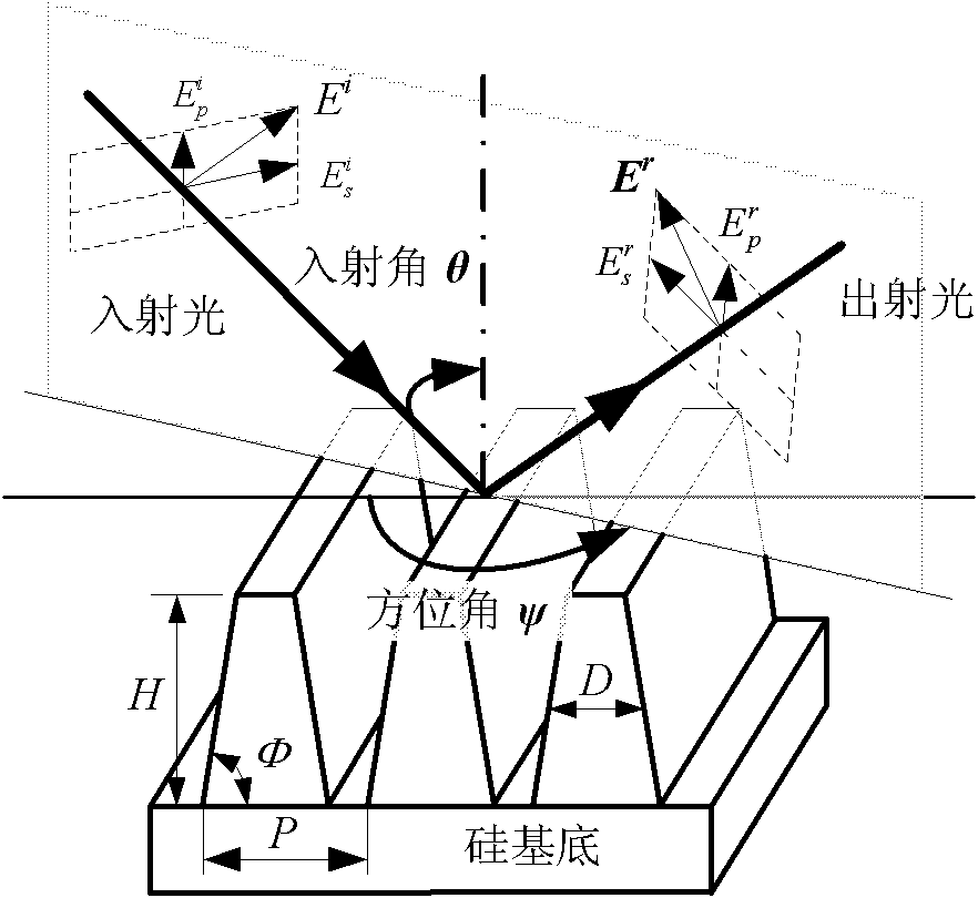
[0025] (1) After the incident beam with a wavelength ranging from ultraviolet to near-infrared is subjected to spectral splitting, polarization, and pre-phase compensation, an elliptically polarized beam is obtained and projected onto the surface of the structure to be measured containing nanostructures.

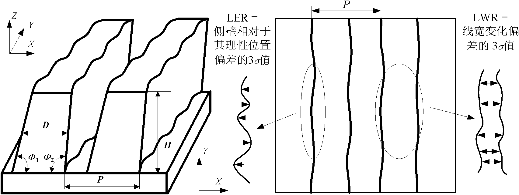
[0026] The wavelength of the incident beam can be selected from ultraviolet, visible light, near-infrared bands or a combination thereof according to the geometric characteristic scale of the structure to be measured. Taking the measurement process of the one-dimensional pattern array structure in the photolithography process as an example, the structure and shape parameters of the one-dimensional pattern array are as follows: figure 1 shown. The shape parameters of the one-dimensional graphic array structure to be me...


PUM


Abstract

The invention discloses a method and a device thereof for measuring three-dimensional topography of a nano structure, which can simultaneously measure three-dimensional topography parameters such as line width, depth, side corner, line edge roughness, line width roughness and the like of the nano structure. The method comprises the following steps of: performing splitting, polarization and front and back phase compensation on light beams with wavelengths in ultraviolet to near-infrared wave band to obtain elliptical polarized light and projecting the elliptical polarized light for later measurement; acquiring surface reflected zero-level diffraction signals of the to-be-measured structure, and obtaining a measurement Mueller matrix of the nano structure by calculation; and matching the measurement Mueller matrix and a theoretical Mueller matrix, and obtaining a three-dimensional topography parameter value of the to-be-measured nano-scale structure. The device provided by the invention for measuring the three-dimensional topography parameter of the nano structure can provide a non-contact, nondestructive, low-cost and quick measurement means for one-dimensional and two-dimensional sub-wavelength periodic structures in processes of photo-etching, nano impressing and the like of an image transfer-based batch manufacturing method.

Description

technical field [0001] The invention belongs to the nano-manufacturing measurement technology, and specifically relates to a method and device for measuring the three-dimensional shape of a nano-structure. The invention is especially suitable for the line width, depth, side wall angle, and line-edge roughness of a grating structure in photolithography, etching, and nano-imprinting graphics. Measurement of three-dimensional shape parameters such as degree and line width roughness. Background technique [0002] Nano-manufacturing refers to the manufacturing technology in which the characteristic size of the product is on the order of nanometers, that is, the manufacturing technology in which the characteristic size is within 100nm. In order to realize the manipulability, predictability, repeatability and scalability of the nano-manufacturing process, and ensure that the products based on nanotechnology meet the requirements of reliability, consistency, economy and large-scale ...

Claims


Application Information

Patent Timeline
IPC IPC(8): G01B11/00G01B11/24
Inventor 刘世元张传维陈修国
Owner WUHAN EOPTICS TECH CO LTD
Why Eureka
Try Eureka