
Organic semiconductor device

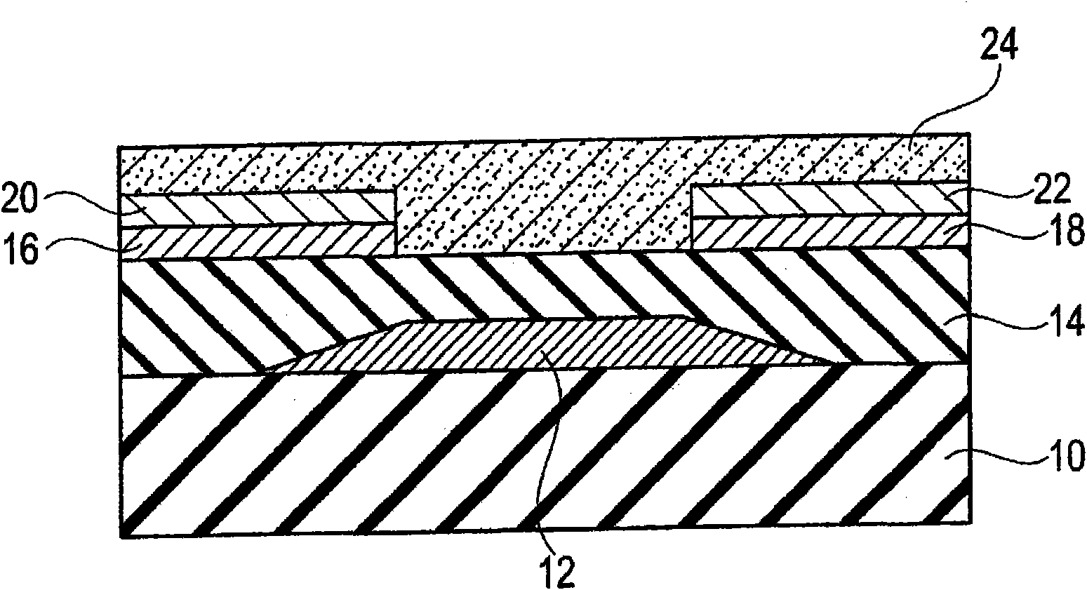
A technology of organic semiconductors and organic semiconductor layers, applied in semiconductor devices, semiconductor/solid-state device manufacturing, transistors, etc., can solve problems such as the inability to control the orientation of organic semiconductor materials, the difficulty in improving the characteristics of organic transistors, and the difficulty in achieving high-performance transistors, etc. , to achieve good orientation control, easy surface modification, and high hole injection ability

Inactive Publication Date: 2010-11-10
ROHM CO LTD
View PDF2 Cites 2 Cited by
  • Summary
  • Abstract
  • Description
  • Claims
  • Application Information

AI Technical Summary

Problems solved by technology

[0004] In addition, tantalum oxide (tantalum oxide: Ta 2 o 5 ) film has high dielectric constant (the relative dielectric constant of the bulk material is 25), therefore, when it is used as a gate insulating film of a transistor, it may cause a large reduction in gate driving voltage; and therefore which has 2 o 5 Due to the hysteresis characteristics caused by the internal defects of the film itself and bonding, it is impossible to use the tantalum oxide film as a stable gate insulating film, and it is difficult to achieve high performance transistors
[0005] In addition, when a tantalum oxide film is used as a gate insulating film of an organic transistor, surface modification becomes extremely difficult, and good orientation control of the organic semiconductor material cannot be performed, and it is difficult to improve the characteristics of the organic transistor (low voltage drive, high drive current)

Method used


Image

  • Organic semiconductor device
  • Organic semiconductor device
  • Organic semiconductor device

Examples


no. 1 Embodiment approach

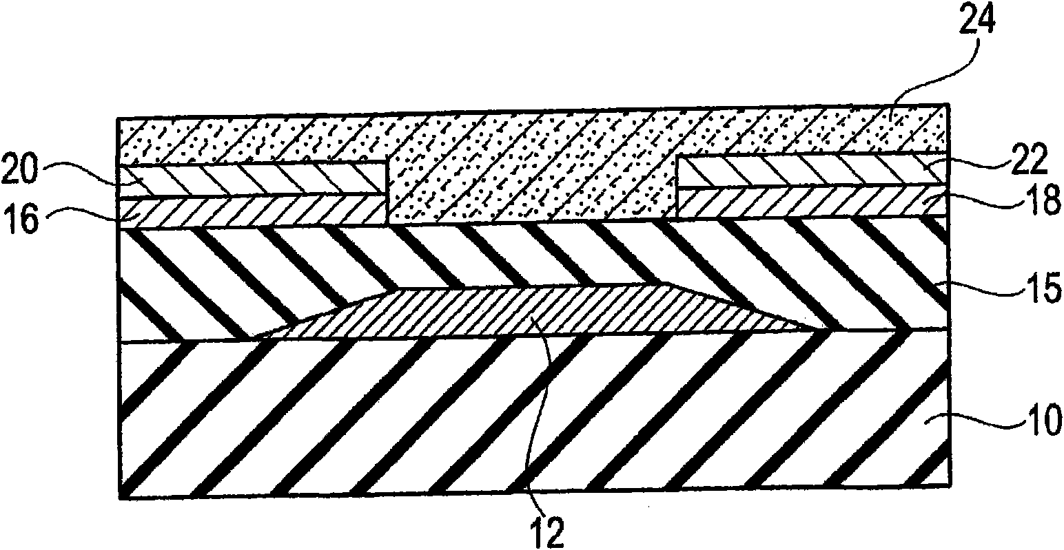
[0105] Figure 5 A schematic cross-sectional structure of the organic semiconductor device according to the first embodiment of the present invention is shown. also, Image 6 and Figure 7 The drain current I of the organic semiconductor device according to the first embodiment of the present invention is shown respectively. D - Drain voltage V D Characteristic example, drain current I D - Gate voltage V G Feature example.

[0106] like Figure 5 As shown, the structure of the organic semiconductor device according to the first embodiment of the present invention has an organic thin film transistor, and the organic thin film transistor has: a substrate 10; a gate 12 arranged on the substrate 10; a gate insulating layer arranged on the gate 12 film 15; the gate insulating film 17 arranged on the gate insulating film 15; the source electrode (16, 20) and the drain (18, 22); and, the organic semiconductor layer 24 provided between the source (16, 20) and the drain (18, 22...

no. 2 Embodiment approach

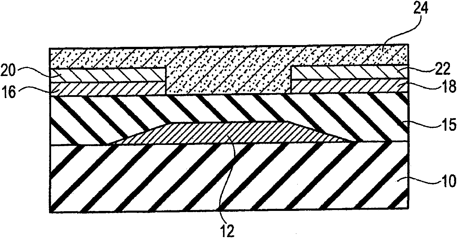
[0148] Figure 8 A schematic cross-sectional structure of the organic semiconductor device according to the second embodiment of the present invention is shown. also, Figure 9 and Figure 10 The drain currents I of the organic semiconductor device according to the second embodiment of the present invention are respectively shown D - Drain voltage V D Characteristic example, drain current I D - Gate voltage V G Feature example.

[0149] like Figure 8 As shown, the organic semiconductor device according to the second embodiment of the present invention has a structure of an organic thin film transistor including: a substrate 10 ; a gate electrode 12 provided on the substrate 10 ; a gate insulator provided on the gate electrode 12 film 15; the gate insulating film 170 provided on the gate insulating film 15; the source electrode (16, 20) and drain electrodes (18, 22); and an organic semiconductor layer 24 provided between the source electrodes (16, 20) and the drain ele...

no. 3 Embodiment approach

[0185] Figure 15 A schematic cross-sectional structure of an organic semiconductor device according to a third embodiment of the invention is shown.

[0186] like Figure 15As shown, the organic semiconductor device according to the third embodiment of the present invention has an organic thin film transistor, and the organic thin film transistor includes: a substrate 10; a gate 12 disposed on the substrate 10; a gate insulating film 13 disposed on the gate 12; The gate insulating film 15 disposed on the gate insulating film 13; the gate insulating film 170 disposed on the gate insulating film 15; the metal layers 16, 18 and the metal layer 20, disposed on the gate insulating film 170 The source (16, 20) and the drain (18, 22) formed by the laminated structure of 22; The organic semiconductor layer 24.

[0187] In addition, the gate insulating film 15 can be made of, for example, a tantalum oxide film with a thickness of 100 nm or less, and the gate insulating films 13 and...


PUM


Abstract

Provided is an organic semiconductor device suitable for integration by having an organic thin film transistor of low voltage drive and high drive current. The organic semiconductor device is provided with the organic thin film transistor. The thin film transistor is provided with a substrate (10); a gate electrode (12) arranged on the substrate (10); a first gate insulating film (15) arranged on the gate electrode (12); a second gate insulating film (17) arranged on the first gate insulating film (15); source electrodes (16, 20) and drain electrodes (18, 22) arranged on the second gate insulating film (17) and are composed of a laminated structure of first metal layers (16, 18) and second metal layers (20, 22); and an organic semiconductor layer (24) arranged between the source electrodes (16, 20) and the drain electrodes (18, 22) on the gate insulating film (17). The first gate insulating film (15) is composed of an insulating film having a dielectric constant higher than that of the second gate insulating film (17), the second gate insulating film (17) is composed of a silicon oxide film thinner than the first gate insulating film (15), and a laminated type gate insulating film structure is provided as a whole.

Description

technical field [0001] The present invention relates to an organic semiconductor device, in particular to a laminated structure with a high dielectric constant insulating film and an extremely thin oxide film, or using a material with a large work function for source / drain electrodes to improve transistor performance organic semiconductor devices. Background technique [0002] As a circuit element using an organic semiconductor, a circuit element that can stably maintain the properties of an organic semiconductor for a long time, exhibit high durability against various external stresses, shocks, and the like, and has excellent reliability ( For example, see Patent Document 1). In the circuit element of Patent Document 1, there is provided a circuit element obtained by forming a circuit portion including an organic semiconductor on a substrate, and the circuit element is characterized by having a circuit portion for surrounding the circuit portion so that the circuit portion...

Claims


Application Information

Patent Timeline
Patent Type & Authority Applications(China)
IPC IPC(8): H01L29/786H01L51/05
CPCH01L51/0529H01L51/0545H01L51/105H10K10/474H10K10/84H10K10/466
Inventor 奥良彰
Owner ROHM CO LTD
Learn More