TFT-LCD (Thin Film Transistor Liquid Crystal Display) array base plate and manufacturing method thereof

The technology of an array substrate and manufacturing method, which is applied in the field of TFT-LCD array substrate and its manufacturing, can solve problems such as poor disconnection, achieve the effects of not affecting production capacity, improving aperture ratio and display brightness, and reducing defective gate line disconnection

Inactive Publication Date: 2010-11-17
BEIJING BOE OPTOELECTRONCIS TECH CO LTD
View PDF0 Cites 7 Cited by
  • Summary
  • Abstract
  • Description
  • Claims
  • Application Information

AI Technical Summary

Problems solved by technology

[0005] The purpose of the present invention is to provide a TFT-LCD array substrate and its manufacturing method, which can effectively solve the technical defects such as poor disconnection in the preparation process of the TFT-LCD array substrate in the prior art.

Method used


Image

  • TFT-LCD (Thin Film Transistor Liquid Crystal Display) array base plate and manufacturing method thereof
  • TFT-LCD (Thin Film Transistor Liquid Crystal Display) array base plate and manufacturing method thereof
  • TFT-LCD (Thin Film Transistor Liquid Crystal Display) array base plate and manufacturing method thereof

Examples


Embodiment Construction

[0063] The technical solutions of the present invention will be described in further detail below with reference to the accompanying drawings and embodiments.

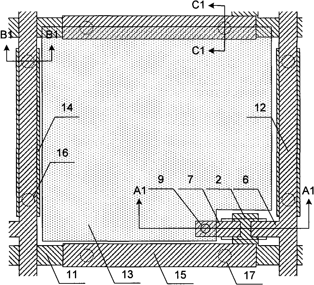
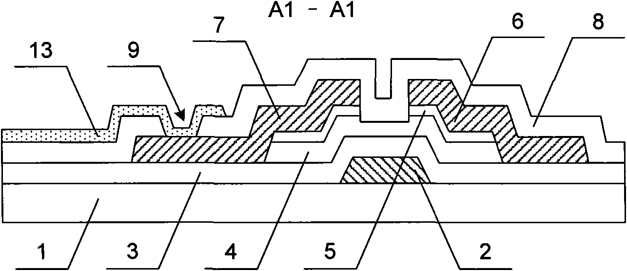
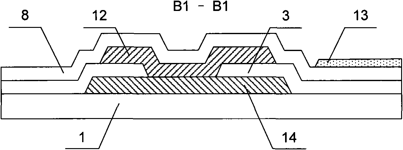
[0064] figure 1 It is a plan view of the first embodiment of the TFT-LCD array substrate of the present invention, reflecting the structure of a pixel unit, figure 2 for figure 1 The cross-sectional view of A1-A1 in the middle, image 3 for figure 1 The sectional view of B1-B1 direction in the middle, Figure 4 for figure 1 Sectional view of C1-C1 in the middle. Such as Figure 1 to Figure 4 As shown, the main structure of the TFT-LCD array substrate in this embodiment includes several gate lines 11 and data lines 12, and the gate lines 11 and data lines 12 perpendicular to each other define several pixel areas, and each pixel area is formed with pixels The electrode 13 and the thin film transistor, in each pixel area, the first connection electrode 14 connected to the data line 12 is arranged under the data li...


PUM


Abstract

The invention relates to a TFT-LCD (Thin Film Transistor Liquid Crystal Display) array base plate and a manufacturing method thereof. The array base plate comprises a grid line and a data line, wherein a pixel electrode and a thin film transistor are formed in a pixel region limited by the grid line and the data line, and a connection electrode forming a double-layer structure for the grid line and / or the data line is also arranged in the pixel region. The manufacturing method comprises the following steps of: forming a figure including the grid line, the data line, an active layer, a source electrode and a drain electrode, wherein the grid line and / or the data line is in the double-layer structure; depositing a passivation layer to form a figure including the pixel electrode, wherein a passivation layer through hole is positioned in the same position of the drain electrode; and depositing a transparent conductive thin film to form a figure including the pixel electrode, wherein the pixel electrode is connected with the drain electrode through the passivation layer through hole. The TFT-LCD array base plate effectively reduces bad line breakage of the grid line and the data line to greatly improve the quality and the yield of the product, simultaneously improves the size of capacitance storage in unit area and is beneficial to improving the opening rate and the display luminance of a TFT-LCD.

Description

technical field [0001] The invention relates to a liquid crystal display and a manufacturing method thereof, in particular to a TFT-LCD array substrate and a manufacturing method thereof. Background technique [0002] Thin Film Transistor Liquid Crystal Display (TFT-LCD for short) has the characteristics of small size, low power consumption, and no radiation. It has developed rapidly in recent years and occupies a dominant position in the current flat panel display market. The liquid crystal panel is one of the most important components in TFT-LCD, mainly including the array substrate and the color filter substrate that are boxed together and the liquid crystal is sandwiched between them. The array substrate includes several gate lines and data lines which are insulated and intersect with each other. The gate lines and data lines define several pixel areas, and each pixel area is formed with a pixel electrode and a thin film transistor. The preparation of the TFT-LCD array ...

Claims


Application Information

Patent Timeline
Patent Type & Authority Applications(China)
IPC IPC(8): H01L27/12H01L23/528H01L21/84H01L21/768G02F1/1368
Inventor 徐超张弥刘竞
Owner BEIJING BOE OPTOELECTRONCIS TECH CO LTD
Why Eureka
Try Eureka