
Pre-oxidation method of semiconductor packaging and routing surface and pre-oxidation layer structure thereof

A technology of pre-oxidation treatment and pre-oxidation layer, which is applied in the direction of semiconductor devices, semiconductor/solid-state device manufacturing, semiconductor/solid-state device components, etc. issues such as life expectancy

Inactive Publication Date: 2010-11-24
ASE ASSEMBLY & TEST SHANGHAI
View PDF3 Cites 5 Cited by
  • Summary
  • Abstract
  • Description
  • Claims
  • Application Information

AI Technical Summary

Problems solved by technology

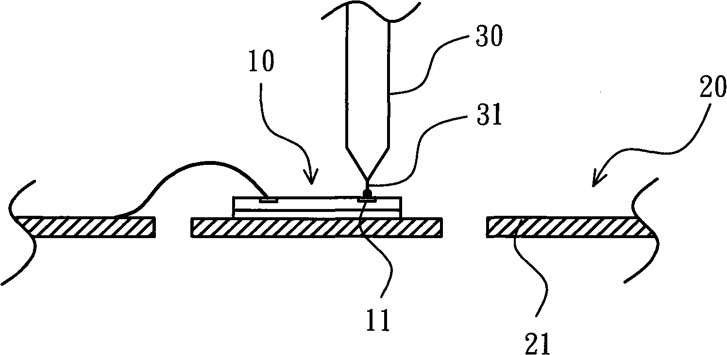
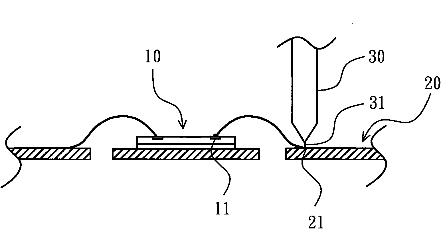
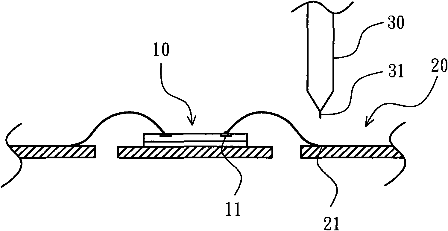
[0006] However, after the wire bonding process of the wire 31 and before and after the packaging process, the wire 31 and the soldering points 11, 12 (chip bonding pads, contacts of inner pins) are exposed to the general environment. In or sealed in the sealing material P, the surface of the wires 31 and the soldering points 11, 12 (chip pads, contacts of inner pins) may be due to moisture or halogen ions in the air and the sealing material P Corrosion reaction resulting in severe defects
During the packaging process, the corrosion defects of the wires 31 and the solder joints 11, 12 may seriously affect the soldering quality of the wire bonding portion, and reduce the yield rate of the semiconductor package.
Even if it does not lead to defective products, the reliability and service life of semiconductor packaging products after leaving the factory will still be affected

Method used


Image

  • Pre-oxidation method of semiconductor packaging and routing surface and pre-oxidation layer structure thereof
  • Pre-oxidation method of semiconductor packaging and routing surface and pre-oxidation layer structure thereof
  • Pre-oxidation method of semiconductor packaging and routing surface and pre-oxidation layer structure thereof

Examples


Embodiment Construction

[0025] In order to make the above-mentioned purposes, features and advantages of the present invention more obvious and understandable, the preferred embodiments of the present invention will be specifically cited below, together with the accompanying drawings, for a detailed description as follows:

[0026] The first embodiment of the present invention provides a method for pre-oxidation treatment of the wire bonding surface of a semiconductor package. First, two wire bonding processes are performed, followed by pre-oxidation treatment, and finally the packaging process. Please refer to Figures 3A to 7 As shown, the pre-oxidation treatment method of the semiconductor package wire bonding surface includes the following steps: providing a wire 40 and a wire bonding surface 50, 50', and one end of the wire 40 is soldered and bonded to the wire bonding surface 50 , 50', forming a wire bonding part 60, 60'; providing an oxidizing gas G in the wire bonding part 60, 60', so that th...


PUM

PropertyMeasurementUnit
Thicknessaaaaaaaaaa

Abstract

The invention discloses a pre-oxidation method of a semiconductor packaging and routing surface and a pre-oxidation layer structure thereof. The pre-oxidation method comprises the following steps of: providing a lead and a routing joint surface, wherein one end of the lead is welded and combined to the routing joint surface to form a routing and combining part; providing an oxidizing gas for the routing and combining part to ensure that a pre-oxidation layer is formed on the routing joint surface on the routing and combining part and / or the surface of the lead; and packaging the lead, the routing joint surface, the pre-oxidation layer and the routing and combining part by utilizing a sealing glue material. Because the routing joint surface and / or the surface of the lead have / has the pre-oxidation layer, when the packaging procedure is carried out, the pre-oxidation layer can prevent the lead and / or the routing joint surface from being corroded, so that the risk of generating oxidation defects in the packaging procedure can be reduced so as to improve the welding quality of the routing and combining part and effectively improve the yield of semiconductor packaging.

Description

【Technical field】 [0001] The present invention relates to a method for pre-oxidation treatment of the bonding surface of a semiconductor package and its pre-oxidation layer structure, in particular to a semiconductor package in which the wire and / or the bonding surface of the semiconductor package are subjected to pre-oxidation treatment in the bonding process of the semiconductor package The pre-oxidation treatment method and the pre-oxidation layer structure of the wire bonding surface. 【Background technique】 [0002] In the existing manufacturing process of semiconductor packaging, the semiconductor wafer is usually obtained first and the wafer test is carried out on it. After passing the test, the semiconductor wafer will then be cut into several semiconductor chips, and each semiconductor chip will be glued on the Leadframe (leadframe) or substrate (substrate) for wire bonding (wire bonding) procedures. Wire bonding technology is widely used in the electrical connectio...

Claims


Application Information

Patent Timeline
IPC IPC(8): H01L21/60H01L23/488H01L23/49
CPCH01L2224/92247H01L2224/92H01L2924/0105H01L2924/01082H01L2224/78301H01L2924/01047H01L24/78H01L2224/48465H01L2224/32245H01L2224/48247H01L24/85H01L2924/01005H01L2924/01033H01L2924/01029H01L2924/01028H01L2924/01013H01L2224/73265H01L2224/85181H01L2924/181H01L2224/48091H01L2224/8592H01L24/73H01L2224/85H01L2224/78H01L2924/00014H01L2924/00H01L2924/00012
Inventor 王德峻吕岱烈杜嘉秦
Owner ASE ASSEMBLY & TEST SHANGHAI
Learn More