Semiconductor device

A semiconductor and device technology, applied in the field of semiconductor devices, can solve the problems of increased SGT standby leakage current and increased power consumption

Active Publication Date: 2010-12-01
UNISANTIS ELECTRONICS SINGAPORE PTE LTD
View PDF7 Cites 0 Cited by
  • Summary
  • Abstract
  • Description
  • Claims
  • Application Information

AI Technical Summary

Problems solved by technology

[0014] The present invention was developed in view of the above problems, and its purpose is to solve the problem of increased power consumption caused by the increase of the standby leakage current of SGT, and its purpose is to provide a semiconductor device in which the shape of the source and drain is concave.

Method used


Image

  • Semiconductor device
  • Semiconductor device
  • Semiconductor device

Examples


Embodiment 1

[0201] Embodiment 1 Semiconductor device

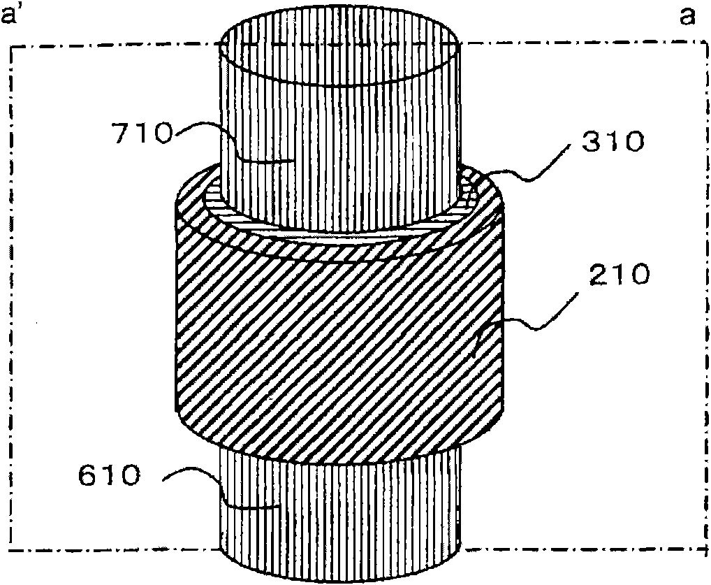
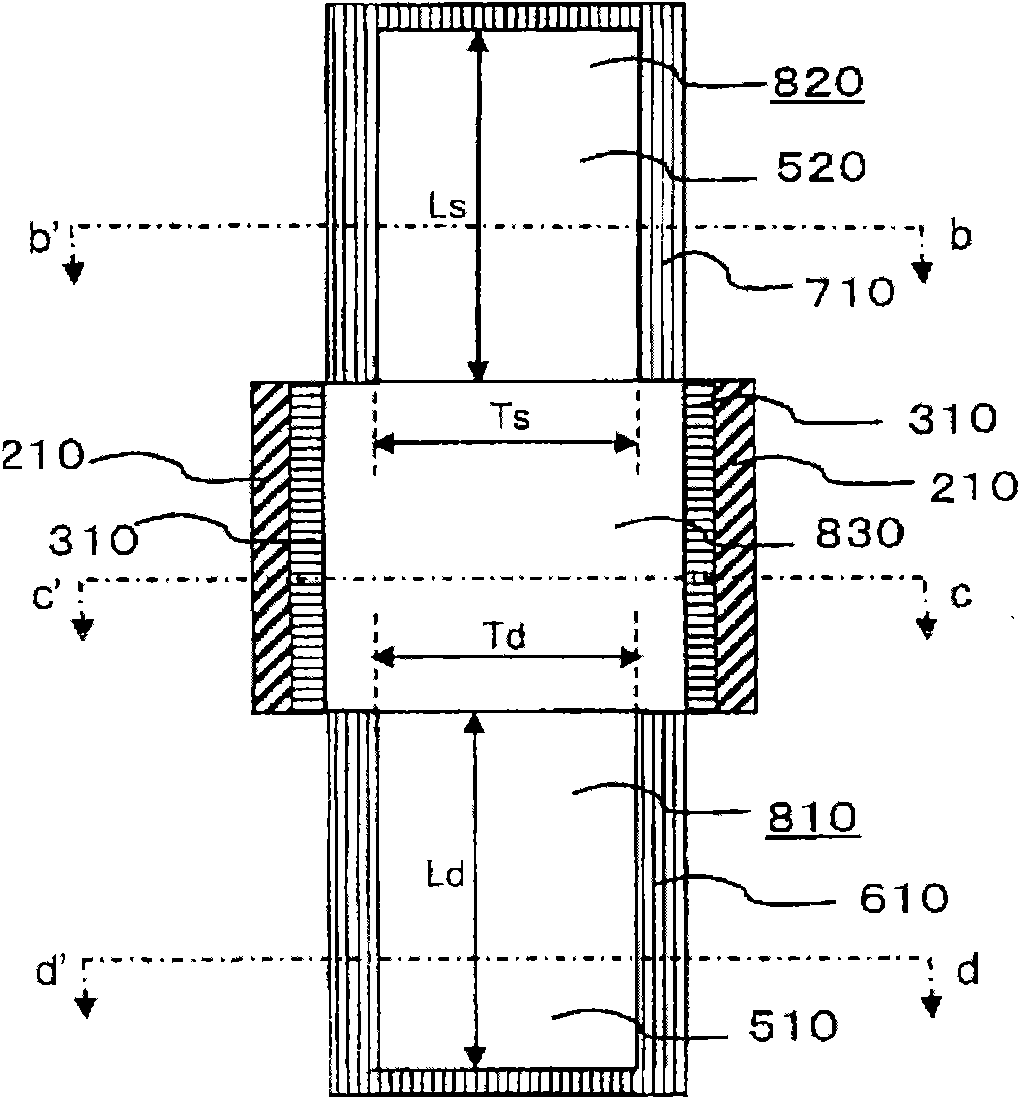
[0202] figure 1 It is a schematic bird's-eye view showing the semiconductor device of Embodiment 1 of the present invention. figure 2 for along figure 1 A schematic cross-sectional view of the cutting line (cut line) a-a'. image 3 for along figure 2 A schematic cross-sectional view of the cutting line b-b'. Figure 4 for along figure 2 A schematic cross-sectional view of the cutting line c-c'. Figure 5 for along figure 2 A schematic cross-sectional view of the cutting line d-d'.

[0203] The semiconductor device of this embodiment includes: a third silicon pillar 830 of the first conductivity type; a first insulator 310 surrounding the side surface of the third silicon pillar 830; a gate 210 surrounding the first insulator 310; a first silicon pillar 810 set On the lower part of the third silicon pillar 830; the second silicon pillar 820 is arranged on the upper part of the third silicon pillar 830; the second conducti...

Embodiment 2

[0227] Embodiment 2 Semiconductor device

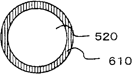
[0228] Figure 8 In order to show that the first conductivity type impurity region 510 formed on the first silicon pillar 810 in the first embodiment is the same second conductivity type as the second conductivity type high-concentration impurity region 610 formed on the first silicon pillar 810 A schematic bird's-eye view of a transistor in the semiconductor device of the present invention in a high-concentration impurity region. Figure 9 for Figure 8 A rough cross-sectional view of the cutting line (cut line) a-a', Figure 10 for Figure 9 A rough cross-sectional view of the cutting line b-b', Figure 11 for Figure 9 A rough profile of the cutting line c-c', Figure 12 for Figure 9 A schematic cross-sectional view of the cutting line d-d'.

[0229] In this embodiment, in order to increase the breakdown voltage, it is more preferable that the first conductive type impurity region 520 included in the second silicon pillar ...

Embodiment 3

[0241] Embodiment 3 Semiconductor device

[0242] Figure 15 In order to show that the first conductivity type impurity region 520 formed on the second silicon pillar 820 in Embodiment 1 is the same second conductivity type as the second conductivity type high-concentration impurity region 710 formed on the second silicon pillar 820 A schematic bird's-eye view of a transistor in the semiconductor device of the present invention in a high-concentration impurity region. Figure 16 for Figure 15 A rough cross-sectional view of the cutting line a-a′, Figure 17 for Figure 16 A rough cross-sectional view of the cutting line b-b', Figure 18 for Figure 16 A rough profile of the cutting line c-c′, Figure 19 for Figure 16 A schematic cross-sectional view of the cutting line d-d'.

[0243] In this embodiment, in order to increase the breakdown voltage, it is more preferable that the first conductive type impurity region 510 included in the first silicon pillar 810 has a la...


PUM

PropertyMeasurementUnit
Lengthaaaaaaaaaa
Film thicknessaaaaaaaaaa
Diameteraaaaaaaaaa

Abstract

Provided is a semiconductor device which is capable of preventing an increase in power consumption of an SGT, i.e., a three-dimensional semiconductor transistor, due to an increase in off-leak current. The semiconductor device comprises: a first-conductive type first silicon pillar: a first dielectric surrounding a side surface of the first silicon pillar; a gate surrounding the dielectric; a second silicon pillar provided underneath the first silicon pillar; and a third silicon pillar provided on a top of the first silicon pillar. The second silicon pillar has a second-conductive type high-concentration impurity region formed in a surface thereof except at least a part of a contact surface region with the first silicon pillar, and a first-conductive type impurity region formed therein and surrounded by the second-conductive type high-concentration impurity region. The third silicon pillar has a second-conductive type high-concentration impurity region formed in a surface thereof except at least a part of a contact surface region with the first silicon pillar, and a first-conductive type impurity region formed therein and surrounded by the second-conductive type high-concentrationimpurity region of the third silicon pillar. The first-conductive type impurity region of each of the second silicon pillar and the third silicon pillar has a length greater than that of a depletion layer extending from a base portion of the second-conductive type high-concentration impurity region of a respective one of the second silicon pillar and the third silicon pillar.

Description

technical field [0001] The present invention relates to a semiconductor device, more specifically, to a semiconductor device of a Surrounding Gate Transistor (SGT) of a three-dimensional semiconductor. Background technique [0002] Through the miniaturization of planar transistors, it has been widely used in the fields of computers or communications, measuring equipment, automatic control devices, and living equipment as a microprocessor (micro) with low power consumption, low cost, and high information processing capability. processor), or ASIC (Application Specific Integrated Circuit, application specific integrated circuit), microcomputer (micro computer), and cheap and large-capacity memory. However, a planar transistor formed in a plane on a semiconductor substrate is formed in a plane. In other words, the source, gate, and drain are horizontally formed on the surface of the silicon substrate. In SGT, the source, gate, and drain are arranged vertically relative to the ...

Claims


Application Information

Patent Timeline
IPC IPC(8): H01L29/78H01L29/06H01L29/08
CPCH01L29/086H01L29/78642H01L29/0878H01L29/42356H01L29/66742H01L29/78618H01L29/7827H01L29/42392H01L21/26586H01L29/66666H01L29/456H01L29/4238
Inventor 舛冈富士雄工藤智彦
Owner UNISANTIS ELECTRONICS SINGAPORE PTE LTD
Why Eureka
Try Eureka