Method o encapsulating a wafer level microdevice

A micro-device, wafer-level technology, applied in the directions of microstructure devices, manufacturing microstructure devices, assembling microstructure devices, etc., can solve the problems of increasing the thickness of wafer stacking, wafer handling problems, etc., to avoid chemical pollution, thin wafers, and transfer. Easy-to-use effects

Active Publication Date: 2010-12-08
XIAN YISHEN OPTOELECTRONICS TECH CO LTD
View PDF3 Cites 6 Cited by
  • Summary
  • Abstract
  • Description
  • Claims
  • Application Information

AI Technical Summary

Problems solved by technology

While this provides physical protection for the microcomponents fabricated on the top side of the silicon wafer from backside thinning, as well as potential mechanical damage and chemical contamination during TSV and interconnect fabrication, it adds significantly to the wafer stack thickness, typically Will grow to twice the thickness of a standard silicon wafer
This creates wafer handling issues during wafer backside preparation for thinning and TSV formation

Method used


Image

  • Method o encapsulating a wafer level microdevice
  • Method o encapsulating a wafer level microdevice
  • Method o encapsulating a wafer level microdevice

Examples


Embodiment 1

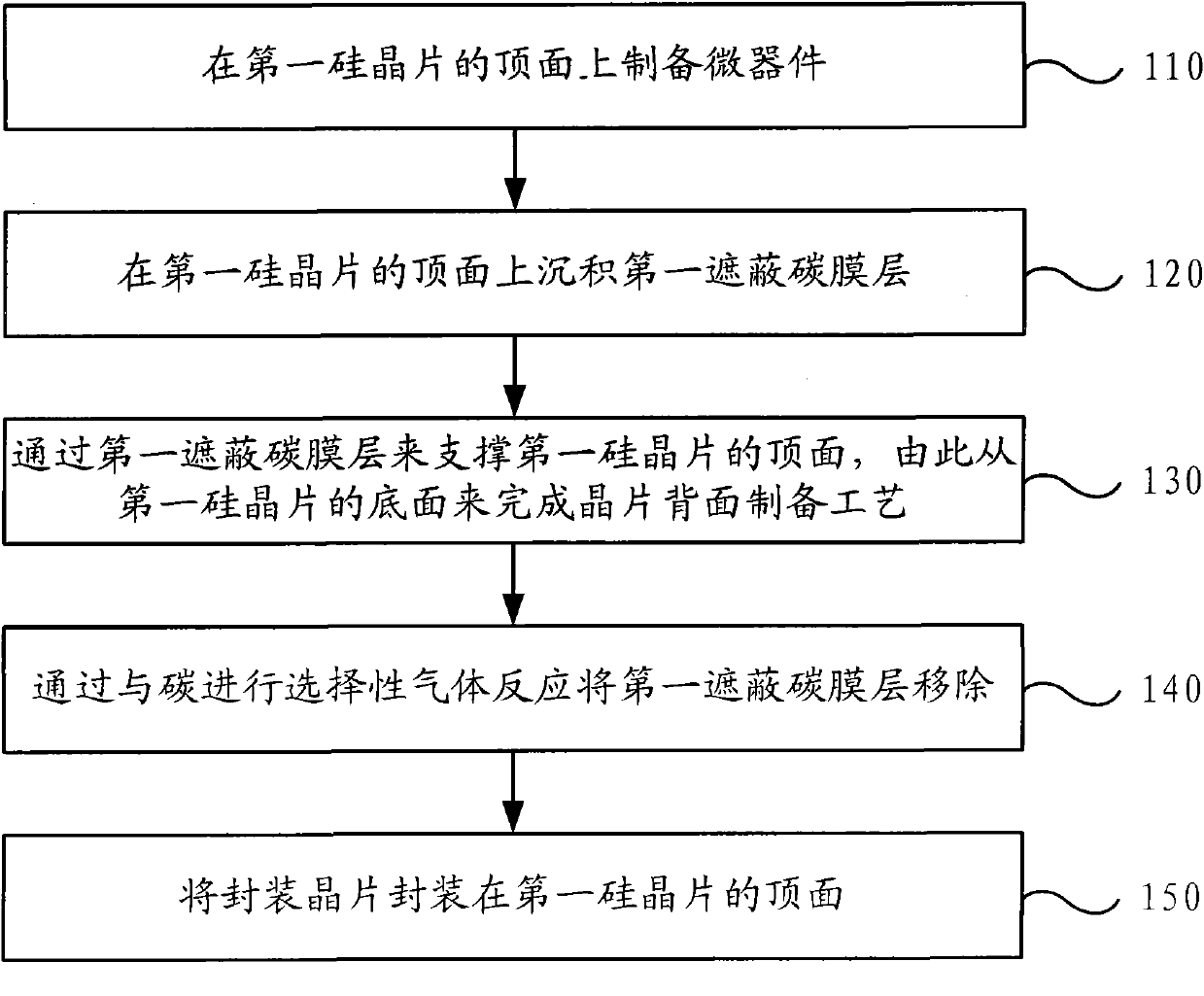
[0029] figure 1 The flow chart of the packaging method of wafer-level micro-device provided for Embodiment 1 of the present invention shows the basic packaging process of the micro-device of the present invention, wherein the details that are known and obvious to the field of wafer-level electronic preparation are ignored and simplified describe. This embodiment specifically includes the following steps:

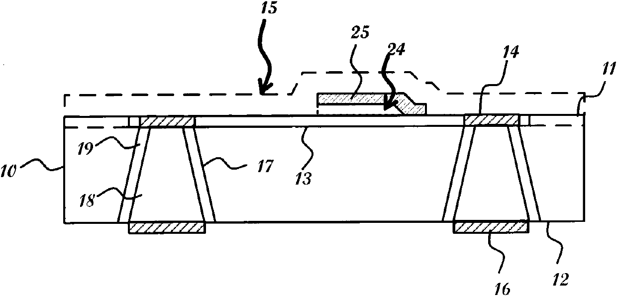
[0030] Step 110, preparing micro-devices 13 on the top surface 11 of the first silicon wafer 10;

[0031] The first silicon wafer 10 is used as a silicon substrate, and any process method in the prior art and / or industrial practice can be used to prepare micro-devices 13, usually a plurality of micro-devices 13 are prepared, and a plurality of micro-devices 13 are in the form of a planar array arrange, such as Figure 2a Shown is the partial structural representation of the micro-device prepared by the first embodiment of the present invention Figure 1 , which exemplari...

Embodiment 2

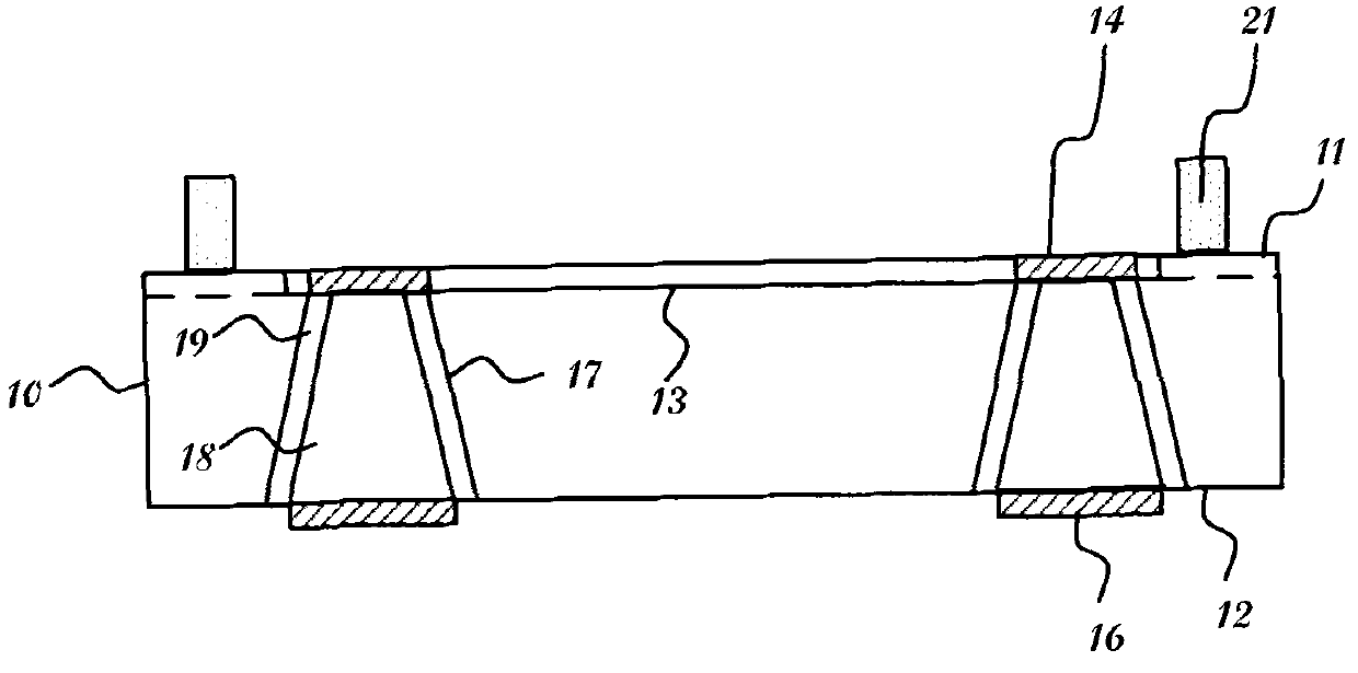
[0052] image 3 It is a flow chart of the packaging method for wafer-level micro-devices provided in Embodiment 2 of the present invention, forming Figure 2e There are many ways of the structure shown, and this embodiment provides a specific implementation way, and packaging the package chip 20 on the top surface 11 of the first silicon chip 10 includes:

[0053] Step 310, prepare a sealing grid 21 on the top surface 11 of the first silicon wafer 10, and the sealing grid 21 surrounds the outside of the micro-device 13, such as Figure 4a As shown, provide sidewalls for the subsequently generated shielding cavity 30;

[0054] Step 320, attach and fix the packaging chip 20 on the sealing grid 21 on the top surface 11 of the first silicon wafer 10, and the packaging chip 20, the sealing grid 21 and the top surface 11 of the first silicon wafer 10 are completely closed and closed. The sealed shielding cavity 30, specifically, the shielding cavity 30 takes the bottom surface of ...

Embodiment 3

[0058] Figure 5 It is a flow chart of the packaging method for wafer-level micro-devices provided in Embodiment 3 of the present invention, forming Figure 2e There are many ways of the structure shown, and this embodiment provides another specific implementation way, and packaging the package chip 20 on the top surface 11 of the first silicon chip 10 includes:

[0059] Step 510, prepare the sealing grid 21 on the surface of the packaging chip 20, such as Image 6 shown;

[0060] Step 520, attach and fix the top surface 11 of the first silicon wafer 10 on the sealing grid 21 of the packaging chip 20, the packaging wafer 20, the sealing grid 21 and the top surface 11 of the first silicon wafer 10 are surrounded to shield the cavity 30. Encapsulate the micro-device 13 in the shielding cavity 30, see Figure 4b shown.


PUM


Abstract

The present invention discloses a method of encapsulating a wafer level microdevice, which includes: fabricating a microdevice on top side of a first silicon wafer; depositing a first capping carbon film on the top side of the first silicon wafer; implementing a backside fabricating process of wafer from bottom side of the first silicon wafer by carrying the top side of the first silicon wafer through the first capping carbon film; removing the first capping carbon film by selective gaseous reaction with carbon; and encapsulating an encapsulation wafer onto the top side of the first silicon wafer. The present invention deposits and removes the first capping carbon film by means of chemical technology, thereby protecting the microdevice on the top side of the first wafer during implementing the backside fabricating process of wafer. The top side does not need to be protected through the encapsulation wafer before implementing the backside fabricating process of wafer, which makes the wafer thinner and convenient to be handled.

Description

technical field [0001] The invention relates to packaging technology, in particular to a packaging method for wafer-level micro devices formed on wafers. Background technique [0002] Many advanced silicon-based microdevices combine various optional microcomponents and basic microelectronic devices on a silicon substrate. The silicon substrate can also be called a silicon wafer. The microcomponents can be mechanical, optical, or chemical. , biological or other types of physical components. Many of these microcomponents need to be encapsulated in tiny or nanoscale cavities formed on the top surface of a silicon substrate. From the formation of microelectronic devices and optional microcomponents, to the formation and packaging of micro-cavities or nano-cavities, micro-devices are preferably able to complete the fabrication process on silicon substrates through a unified wafer-level fabrication process. [0003] However, electronic input and output interface parts are formed...

Claims


Application Information

Patent Timeline
Patent Type & Authority Applications(China)
IPC IPC(8): B81C1/00
CPCB81C1/00333B81C2203/0118
Inventor 河·H·黄
Owner XIAN YISHEN OPTOELECTRONICS TECH CO LTD
Why Eureka
Try Eureka