System and method for extracting parasitic components in analog integrated circuit layout

An integrated circuit and extraction system technology, applied in the fields of instruments, electrical digital data processing, special data processing applications, etc., can solve the problems of special parasitic device extraction, spending a lot of time and energy, etc., and achieve the effect of design optimization

Active Publication Date: 2010-12-22
TSINGHUA UNIV
View PDF3 Cites 17 Cited by
  • Summary
  • Abstract
  • Description
  • Claims
  • Application Information

AI Technical Summary

Problems solved by technology

However, for the design of analog integrated circuits under special processes, such as high-voltage and high-power layout design, some special parasitic structures will be generated due to the high voltage of some nodes in the layout, and these structures cannot be ext

Method used


Image

  • System and method for extracting parasitic components in analog integrated circuit layout
  • System and method for extracting parasitic components in analog integrated circuit layout
  • System and method for extracting parasitic components in analog integrated circuit layout

Examples


Embodiment Construction

[0044] The specific implementation manners of the present invention will be described in detail below in conjunction with the accompanying drawings.

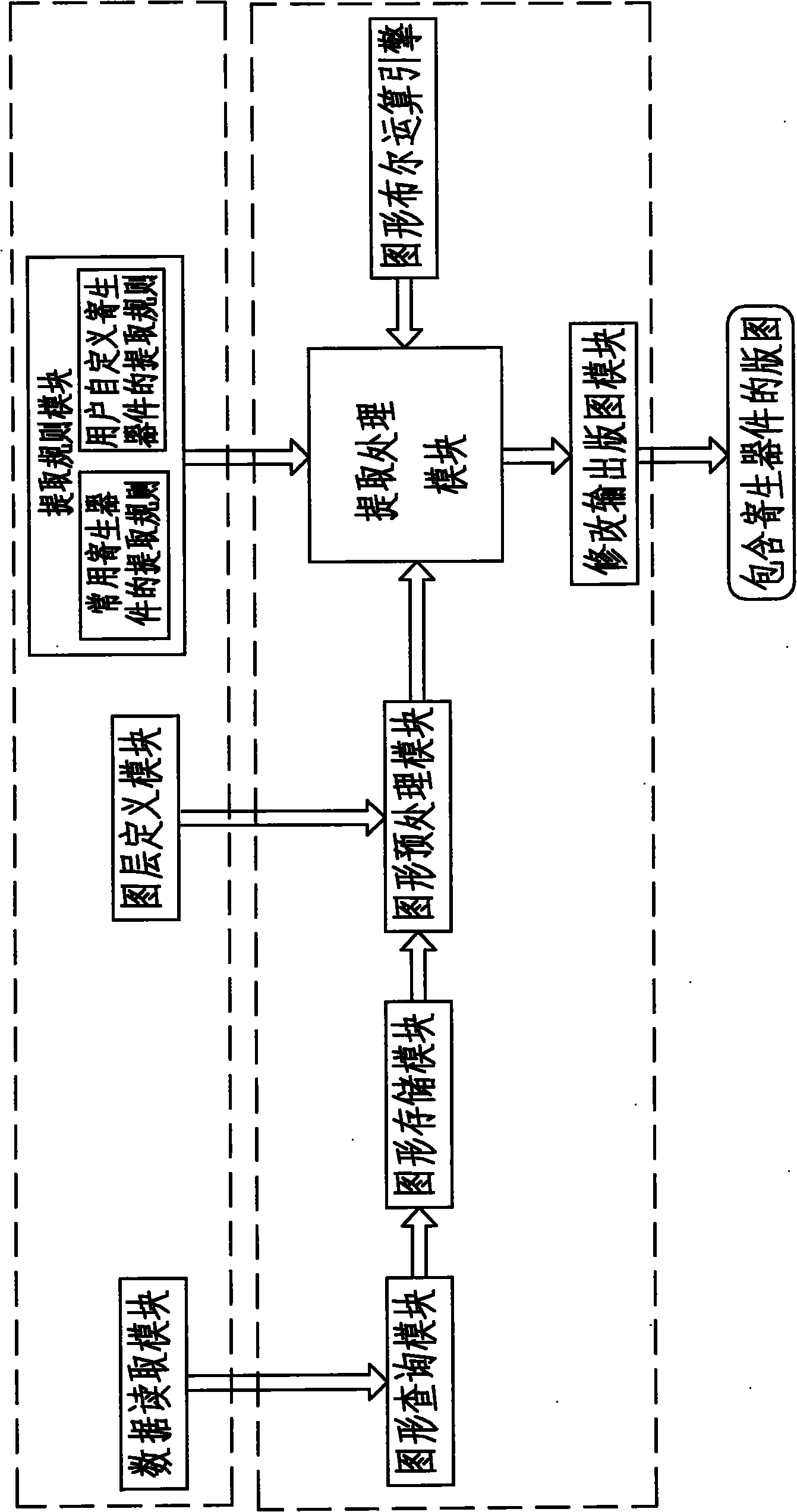
[0045] figure 1 As shown, the principle diagram of the system for extracting special parasitic devices of analog integrated circuit layout according to the present invention. As can be seen from the figure, the present invention consists of the following parts.

[0046] 1. The input includes data reading module, layer definition module and extraction rule module.

[0047] 1.1 Data reading module

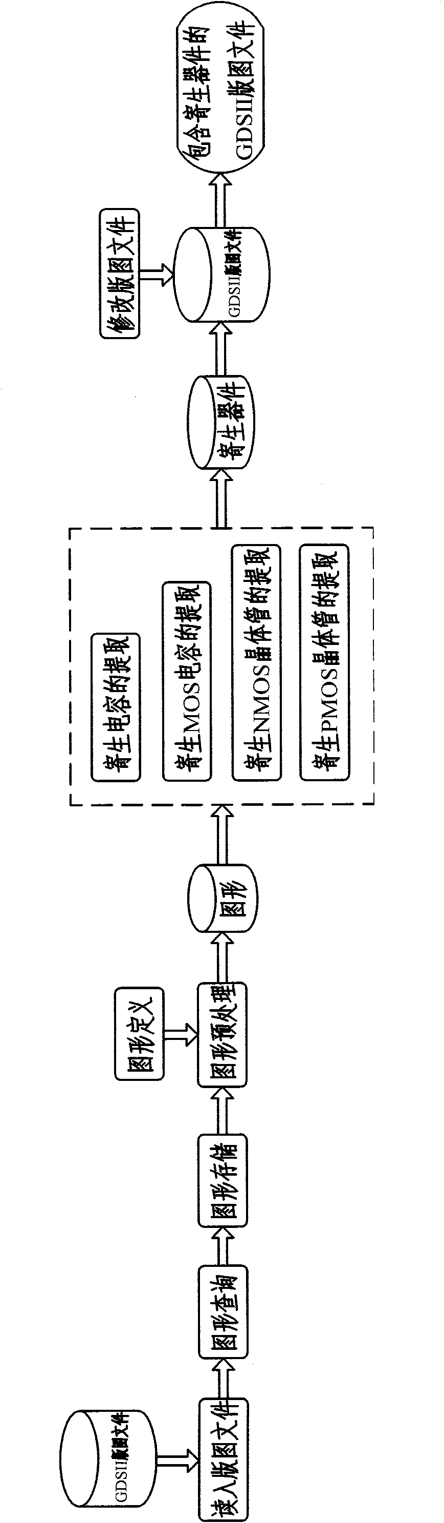
[0048] The standard layout description format is GDSII format. The data reading module of the present invention is based on the OpenAccess (OA) platform, and uses the built-in stream2oa command to convert the GDSII format into the data structure inside the OA. The file in GDSII format is a kind of data stream (stream) for OA. After being converted into the data structure of OA, various API functions provided by OA can be used to op...


PUM


Abstract

The invention discloses a system and method for extracting parasitic components in an analog integrated circuit layout, which is designed to mainly optimize integrated circuit design and extract the parasitic components in different manufacturing processes. The system comprises a data reading module, a layer defining module, a parasitic component extraction rule module and a parasitic component extraction module, wherein the data reading module is used for reading the data of the analog integrated circuit layout; the layer defining module is used for describing the correspondence between geometric layers and physical layers in the layout; the parasitic component extraction rule module is used for making the extraction rule of the parasitic components and generating extraction rule execution files; and the parasitic component extraction module is used for pretreating the received data output by the data reading module, operating and extracting the received data based on the layer defining module and the parasitic component extraction rule module, marking the extracted parasitic components in the analog integrated circuit layout and outputting the analog integrated circuit layout containing the parasitic components. The invention can extract the parasitic components in different manufacturing processes and provide basis for layout optimization design.

Description

technical field [0001] The invention relates to the field of analog integrated circuit design, in particular to the field of integrated circuit design optimization. Background technique [0002] An analog integrated circuit refers to an integrated circuit that integrates analog circuits composed of resistors, capacitors, and transistors on silicon chips to process analog signals. Integrated circuits are designed by designers with the help of Electronic Design Automation (EDA, Electronic Design Automation) tools to design integrated circuit layouts, delivered to integrated circuit manufacturers, through the preparation of circuit masks (Mask), and the oxidation and doping of wafers (Wafer). A series of manufacturing processes such as miscellaneous and photolithography transfer the circuit mask to the wafer to realize its circuit function. However, in the manufacturing process of integrated circuits, different circuit mask layers will form special structures in certain areas....

Claims


Application Information

Patent Timeline
IPC IPC(8): G06F17/50
Inventor 蔡懿慈周强杨建磊
Owner TSINGHUA UNIV
Why Eureka
Try Eureka