Check patentability & draft patents in minutes with Patsnap Eureka AI!

Method for optimizing CMOS imaging sensor layout

An image sensor and layout technology, which is used in instrumentation, semiconductor/solid-state device manufacturing, special data processing applications, etc., can solve the problem of limiting the area of ​​the active area of ​​photodiodes, and achieve the effect of high fill factor and improved image quality.

Active Publication Date: 2010-12-29
SEMICON MFG INT (SHANGHAI) CORP
View PDF0 Cites 1 Cited by
  • Summary
  • Abstract
  • Description
  • Claims
  • Application Information

AI Technical Summary

Problems solved by technology

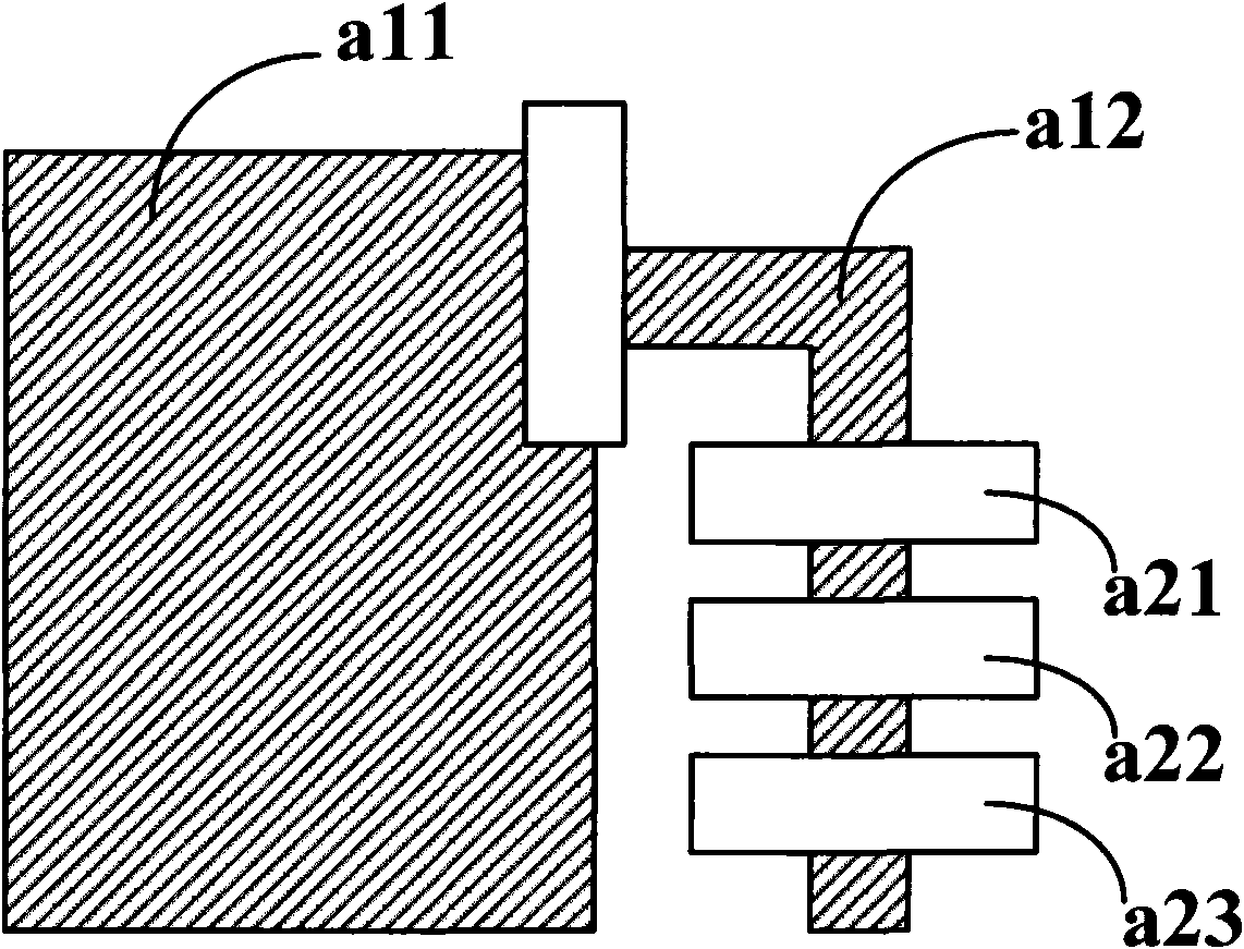
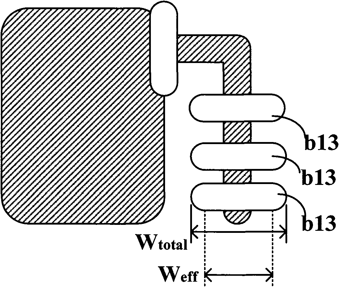
Specifically, the effective width W of the transistor gate electrode region b13 of the pixel unit eff The gate electrode area width W of the transistor is smaller than the actual layout total , taking into account the above factors, the transistor gate electrode area width W of the actual layout total It will be enlarged accordingly in the design to meet the effective gate electrode area width W eff Practical requirements, but this actually limits the area of ​​the active region of the photodiode

Method used


Image

  • Method for optimizing CMOS imaging sensor layout
  • Method for optimizing CMOS imaging sensor layout
  • Method for optimizing CMOS imaging sensor layout

Examples


Embodiment Construction

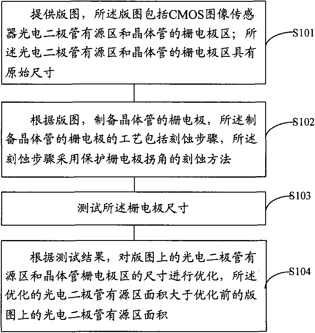
[0014] The present invention provides an embodiment of a method for optimizing the layout of a CMOS image sensor, such as image 3 shown, including the following steps:

[0015] Step S101, providing a layout, the layout including the CMOS image sensor photodiode active area and the gate electrode area of ​​the transistor; the photodiode active area and the transistor gate electrode area have original dimensions;

[0016] Step S102, preparing the gate electrode of the transistor according to the layout, the process of preparing the gate electrode of the transistor includes an etching step, and the etching step adopts an etching method for protecting the corner of the gate electrode;

[0017] Step S103, testing the size of the gate electrode;

[0018] Step S104 , according to the test results, optimize the size of the photodiode active region and the gate electrode region of the transistor on the layout, and the optimized photodiode active region is larger than the photodiode a...


PUM


Abstract

The invention provides a method for optimizing a CMOS imaging sensor layout, which comprises the following steps: providing a layout, wherein the layout comprises a photodiode active area of a CMOS imaging sensor and a gate electrode area of a transistor; the photodiode active area and the gate electrode area of the transistor have the original sizes; manufacturing gate electrodes of the transistor according to the layout, wherein the technology for manufacturing the gate electrodes of the transistor comprises a corrosion step; the corrosion step adopts a corrosion method for protecting gate electrode corners; testing the sizes of the gate electrodes; and optimizing the sizes of the photodiode active area and the gate electrode area of the transistor on the layout according to the testing result, wherein the area of the optimized photodiode active area is larger than that of the photodiode active area before optimization. The CMOS imaging sensor manufactured by the invention meets the technical parameters of the device and has high filling factors, thereby effectively improving the imaging quality of the CMOS imaging sensor.

Description

technical field [0001] The invention relates to the field of semiconductor manufacturing, in particular to a method for optimizing the layout of a CMOS image sensor. Background technique [0002] At present, the charge coupled device (CCD) is the main practical solid-state image sensing device, which has the advantages of low read noise, large dynamic range, and high response sensitivity. The disadvantage of Complementary-Metal-Oxide-Semiconductor (CMOS) technology compatibility is that it is difficult to achieve single-chip integration for image sensors based on charge-coupled devices. The CMOS image sensor (CMOS ImageSensor, CIS) can integrate the pixel array and peripheral circuits on the same chip because of the same CMOS technology. Compared with the charge-coupled device, the CMOS image sensor has small size, light weight, low power Low cost, convenient programming, easy control and low average cost. [0003] A CMOS image sensor includes an array of pixel cells, each...

Claims


Application Information

Patent Timeline
IPC IPC(8): G06F17/50H01L21/8238
Inventor 罗飞邹立
Owner SEMICON MFG INT (SHANGHAI) CORP
Features
  • R&D
  • Intellectual Property
  • Life Sciences
  • Materials
  • Tech Scout
  • Unparalleled Data Quality
  • Higher Quality Content
  • 60% Fewer Hallucinations
Learn More