

Solenoid type heating resistor-containing three-dimensional microheater and manufacturing method thereof
A technology of heating resistance and heating resistance wire, applied in the direction of heating element, heating element shape, ohmic resistance heating parts, etc., to achieve the effects of good controllability, improved performance and high efficiency
- Summary
- Abstract
- Description
- Claims
- Application Information
AI Technical Summary
Problems solved by technology
Method used
Image

Examples
Embodiment 1
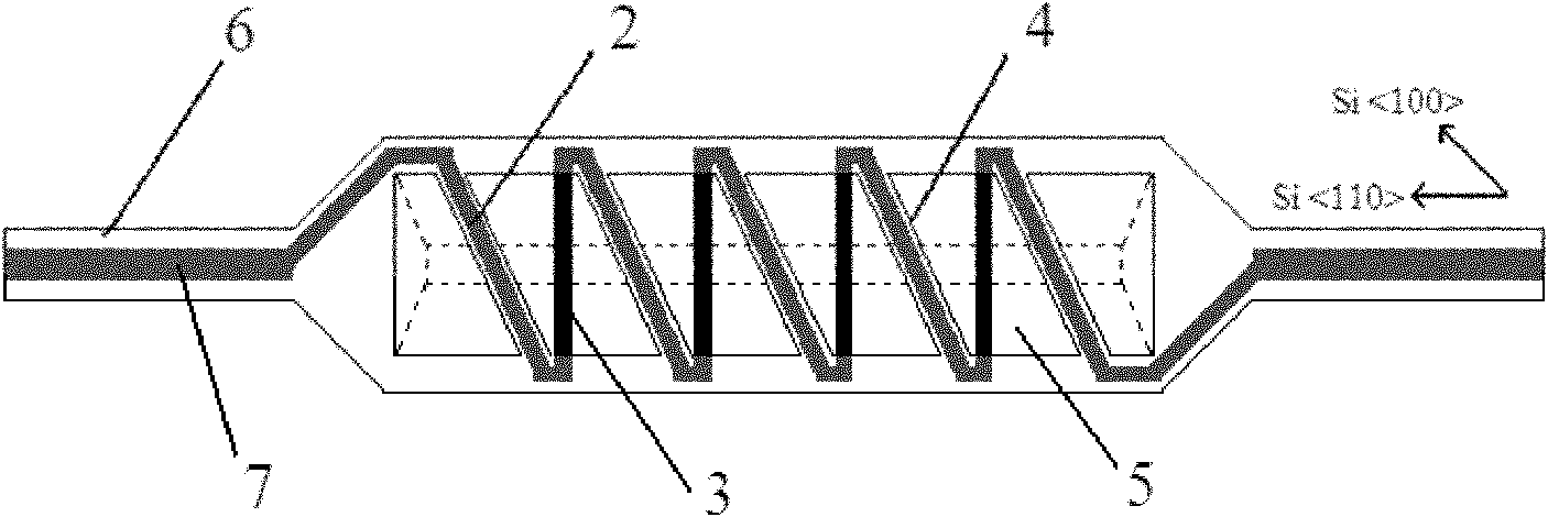
[0033] For the structural diagram of this embodiment, see figure 2 As shown in (a), the specific production method is as follows:
[0034] 1. Substrate selection: choose N-type (100) surface 4-inch silicon wafer as the substrate, resistivity 3-8Ω·cm, silicon wafer thickness 350±10 microns, and trimming angle error <1%.
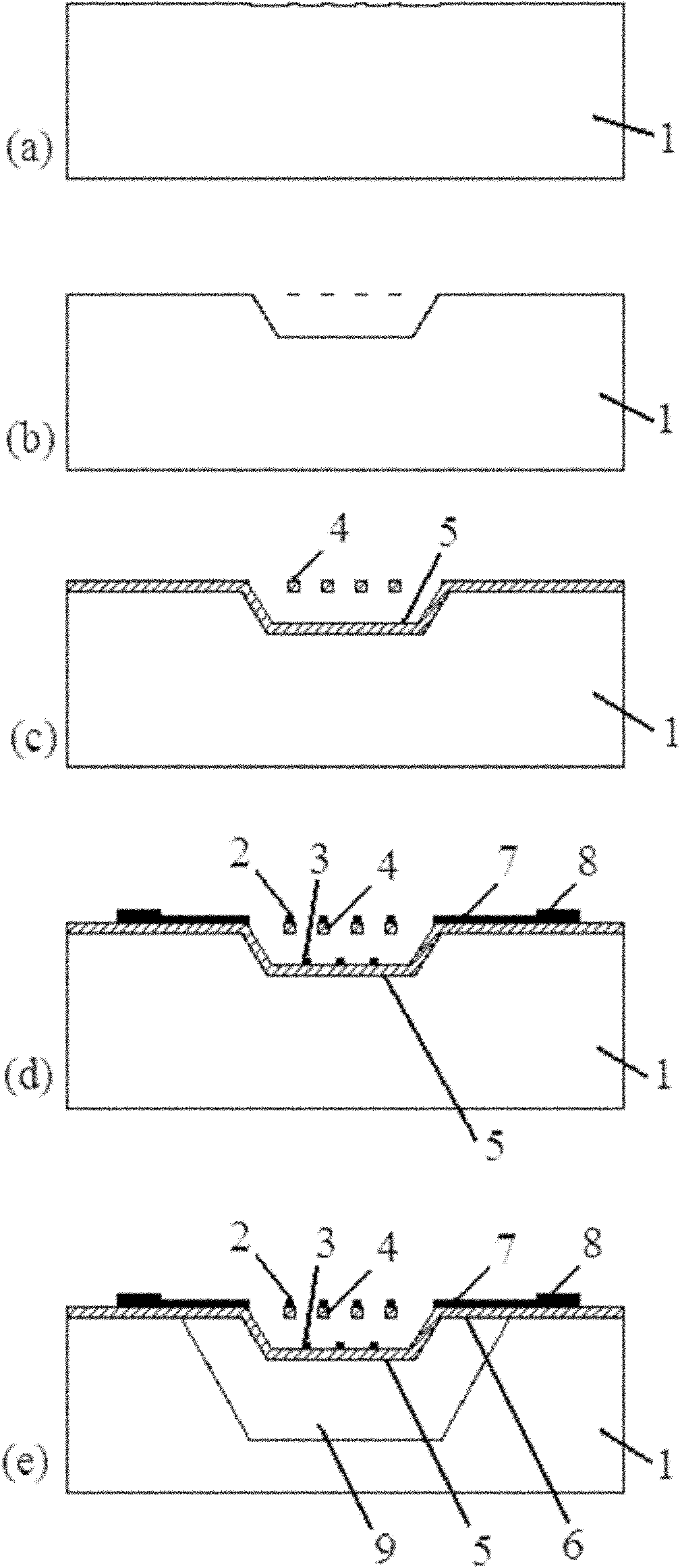
[0035] 2. Make the front etching window used to form the groove structure, and define the silicon oxide layer used to form the upper heating resistance wire support beam: First, use the method of thermal oxidation to grow a layer of silicon oxide with a thickness of 1.0 micron on the surface of the silicon wafer film. Then, the front side photolithography is performed to make a window pattern, and the exposed silicon oxide is completely etched by reactive ion etching (RIE) under the protection of the photoresist to form a front side etching window, and at the same time, the supporting beam for forming the upper heating resistance wire is defined The shape of the ...
Embodiment 2
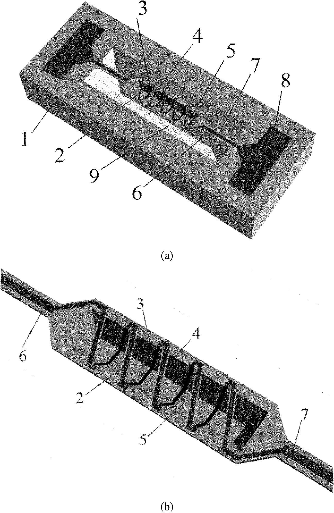
[0042] For the structural diagram of this embodiment, see Figure 4 As shown in (a), the specific production method is as follows:
[0043] 1. Substrate selection: Choose a 4-inch silicon wafer with a P-type (100) surface as the substrate, with a resistivity of 3-8Ω·cm, a silicon wafer thickness of 350±10 microns, and an angle error of trimming <1%.
[0044] 2. Make the front etching window used to form the groove structure, and define the silicon oxide layer used to form the upper heating resistance wire support beam: First, use the thermal oxidation method to grow a layer of silicon oxide with a thickness of 1.0 μm on the surface of the silicon wafer film. Then, the front side photolithography is performed to make a window pattern, and the exposed silicon oxide is completely etched by reactive ion etching (RIE) under the protection of the photoresist to form a front side etching window, and at the same time, the supporting beam for forming the upper heating resistance wire is de...
PUM
| Property | Measurement | Unit |
|---|---|---|
| Total thickness | aaaaa | aaaaa |
| Thickness | aaaaa | aaaaa |
| Resistivity | aaaaa | aaaaa |
Abstract
Description
Claims
Application Information