

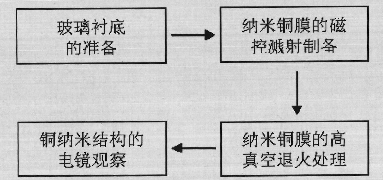
Preparation method of nano copper film-based copper nano structure
A nano-copper and copper nano-technology, applied in the direction of ion implantation plating, metal material coating process, coating, etc., can solve the problems that have not been found in relevant reports, and achieve the effect of simple annealing treatment method and clear mechanism
- Summary
- Abstract
- Description
- Claims
- Application Information
AI Technical Summary
Problems solved by technology
Method used
Image

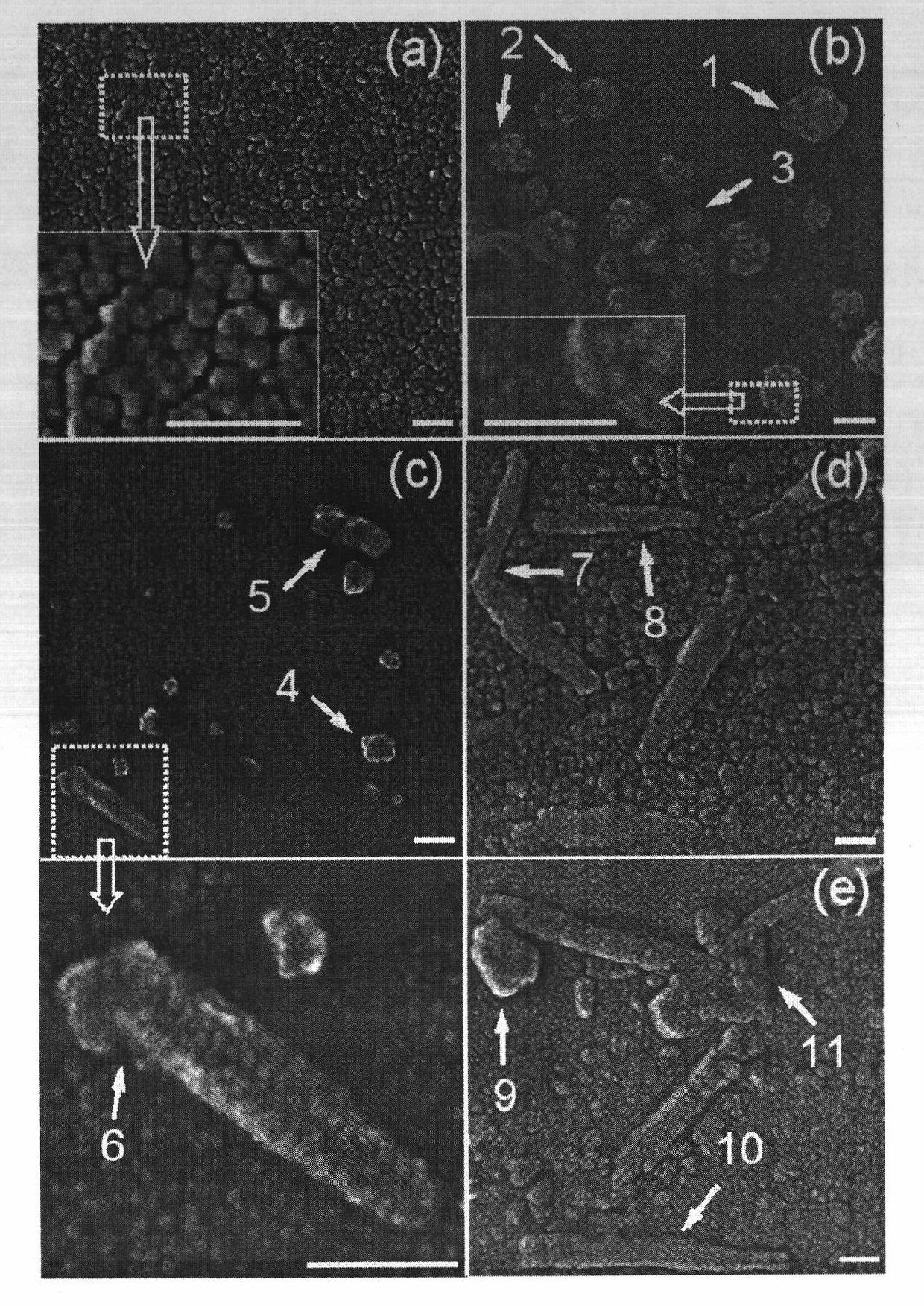

Examples
Embodiment 1
[0020] 1) Preparation of the glass substrate: take a few microscope slides and place them in alcohol for ultrasonic cleaning for 15 minutes, then rinse them repeatedly with deionized water, and then use an electric fan to place the slides front and back at a grazing angle of about 20°. Dry the residual moisture on both sides in one direction, and finally place the glass slide in an oven at 100°C for 15 minutes, and select the cleanest glass slide as the substrate for depositing the nano-copper film;
[0021] 2) Preparation of nano-copper film: place the prepared glass substrate in a magnetron sputtering chamber, install a copper target with a purity of 99.99%, and vacuum the chamber to 5.0×10 -4 Pa, then pass through high-purity Ar gas with a flow rate of 20sccm and a purity of 99.999%, maintain the chamber pressure at 0.5Pa, adjust the sample disk speed to 2r / min, adjust the DC sputtering power to 100W, and remove the baffle at room temperature Start to deposit the copper fil...
PUM
 Abstract
Description
Claims
Application Information