
N-type field effect transistor, metal gate and manufacturing method thereof

A technology of field effect transistors and metal gates, which is applied in the field of semiconductor components with metal gates, can solve problems such as component failure and increase component instability, and achieve the effect of low leakage paths

Active Publication Date: 2012-12-12
TAIWAN SEMICON MFG CO LTD
View PDF0 Cites 1 Cited by
  • Summary
  • Abstract
  • Description
  • Claims
  • Application Information

AI Technical Summary

Problems solved by technology

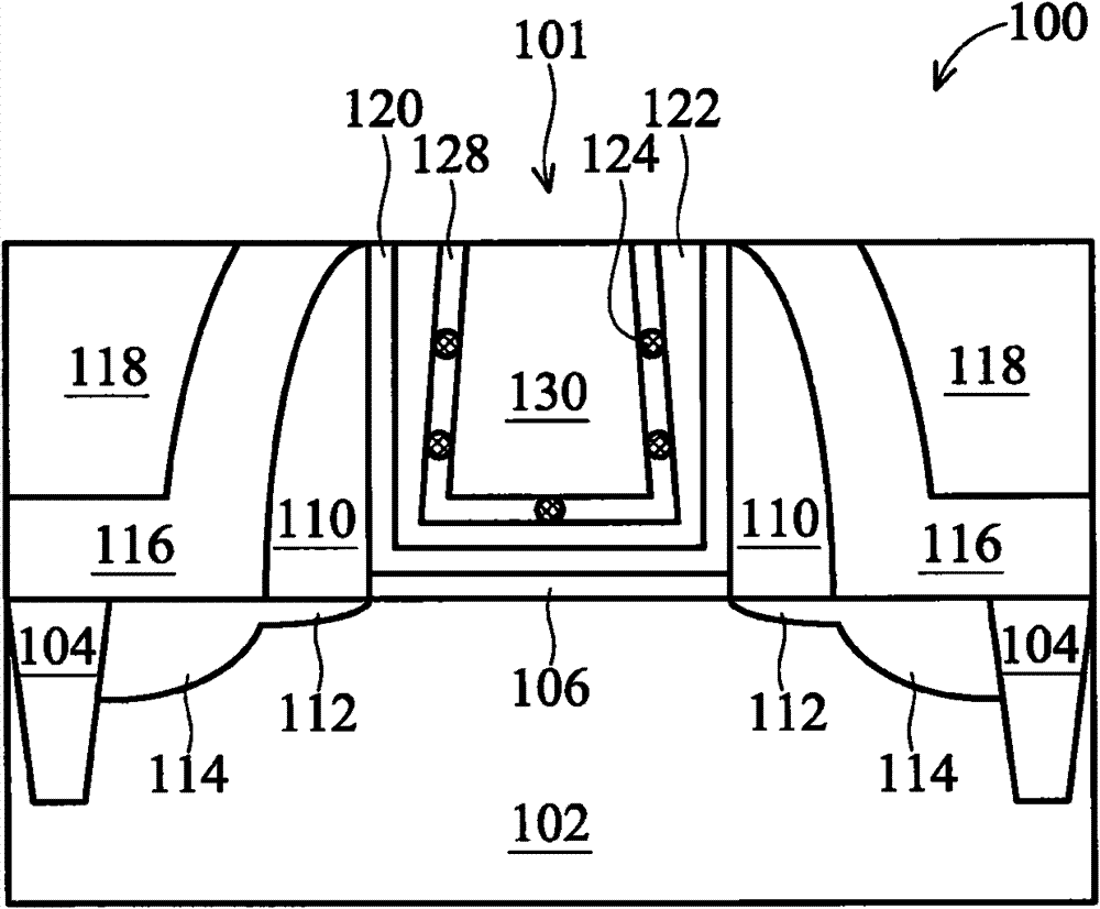
The formation of the intermetallic compound 124 can cause problems, such as forming a leakage path for the gate structure 101, thereby increasing device instability and / or device failure

Method used


Image

  • N-type field effect transistor, metal gate and manufacturing method thereof
  • N-type field effect transistor, metal gate and manufacturing method thereof
  • N-type field effect transistor, metal gate and manufacturing method thereof

Examples


Embodiment Construction

[0033] Various embodiments of the present invention will be described below. In various examples in this specification, repeated element symbols may appear to simplify the description, but this does not mean that there is any specific relationship between the various embodiments and / or the drawings. . Furthermore, when it is mentioned that a certain element is located "on" or "over" another element, it may mean that the two elements are in direct contact or that other elements or film layers are interposed therebetween. In order to simplify the drawings and highlight the features of the present invention, various components may not be drawn in actual scale.

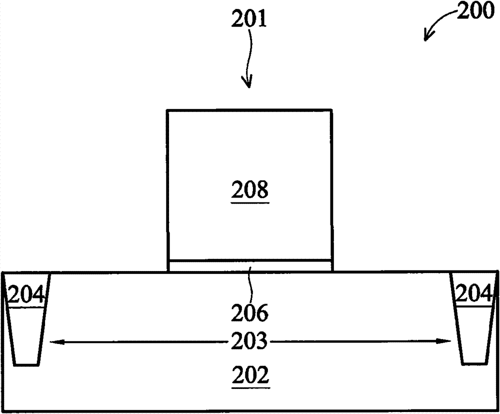
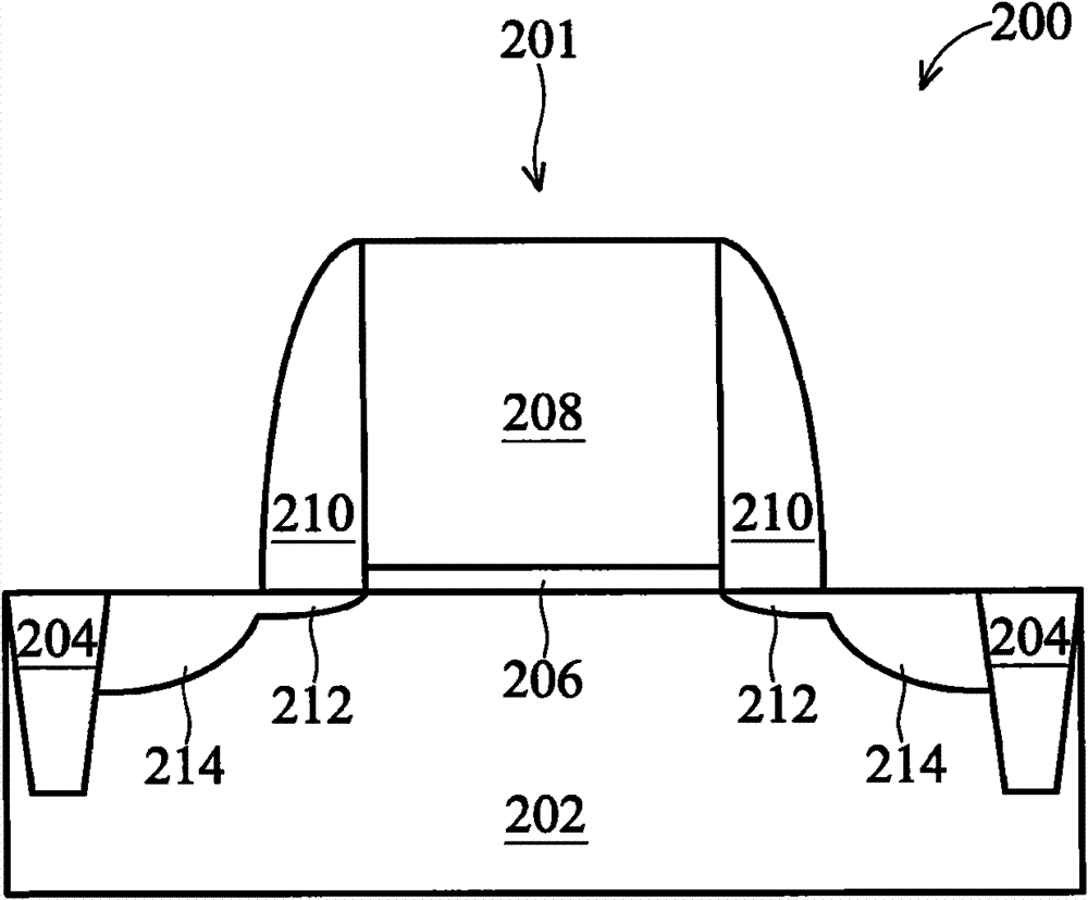
[0034] Please refer to Figure 2A ~ Figure 3 , the semiconductor device 200 and the method 300 will be described together below. Figure 2A ~ Figure 2I A series of cross-sectional views are used to illustrate various stages of the fabrication process of the metal gate structure according to the embodiment of the present...


PUM


Abstract

A semiconductor device structure, for improving the metal gate leakage within the semiconductor device. A structure for a metal gate electrode for a n-type Field Effect Transistor includes a capping layer; a first metal layer comprising Ti and Al over the capping layer; a metal oxide layer over the first metal layer; a barrier layer over the metal oxide layer; and a second metal layer over the barrier layer.

Description

technical field [0001] The present invention relates to the manufacture of integrated circuits, and more particularly to a semiconductor element having a metal gate. Background technique [0002] As the size of transistors shrinks, the thickness of the gate oxide layer must also be reduced to maintain the performance of the reduced gate length. The high dielectric constant (high-k) gate insulating layer can have a larger actual physical thickness under the same equivalent gate oxide thickness to reduce gate leakage current. [0003] In addition, as technology nodes continue to shrink, some IC designs need to replace traditional polysilicon gates with metal gates to improve device performance. In a process called "gate last", the final metal gate is formed at the last stage to reduce the number of processes (such as high temperature processes) that must be performed after the gate is completed. [0004] figure 1 A partial cross-sectional view of a conventional high-k / metal...

Claims


Application Information

Patent Timeline
Patent Type & Authority Patents(China)
IPC IPC(8): H01L29/40H01L29/78H01L21/336H01L21/28
CPCH01L29/66545H01L29/4966H01L29/7833H01L29/66583H01L29/517
Inventor 张简旭珂吴斯安陈圣文
Owner TAIWAN SEMICON MFG CO LTD
Learn More