Supercharge Your Innovation With Domain-Expert AI Agents!

Phase change random access memory and manufacturing method thereof

A technology of a phase change memory and a manufacturing method, which is applied in the manufacturing of semiconductor/solid state devices, electric solid state devices, semiconductor devices, etc., can solve the problems of reducing the contact area between the bottom electrode 301 and the phase change layer 302, etc., achieve excellent heating effect, improve The effect of read and write speed

Inactive Publication Date: 2012-06-20
SEMICON MFG INT (SHANGHAI) CORP
View PDF1 Cites 0 Cited by
  • Summary
  • Abstract
  • Description
  • Claims
  • Application Information

AI Technical Summary

Problems solved by technology

However, in the existing process, the formation process of the bottom electrode 301 is mainly to form a contact hole in the spacer layer first, and then fill it with metal. The width of the top of the contact hole is always greater than that of the bottom, so the formed bottom electrode 301 is in the shape of an inverted trumpet. , it is difficult to further reduce the contact area between the bottom electrode 301 and the phase change layer 302

Method used


Image

  • Phase change random access memory and manufacturing method thereof
  • Phase change random access memory and manufacturing method thereof
  • Phase change random access memory and manufacturing method thereof

Examples


Embodiment Construction

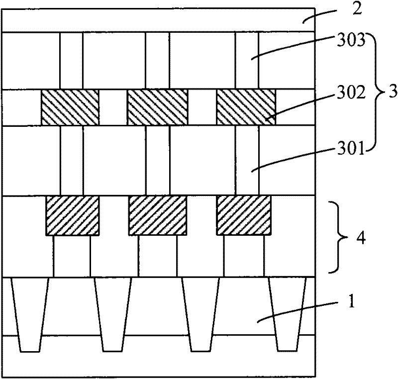
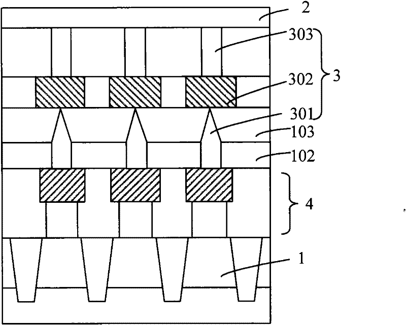
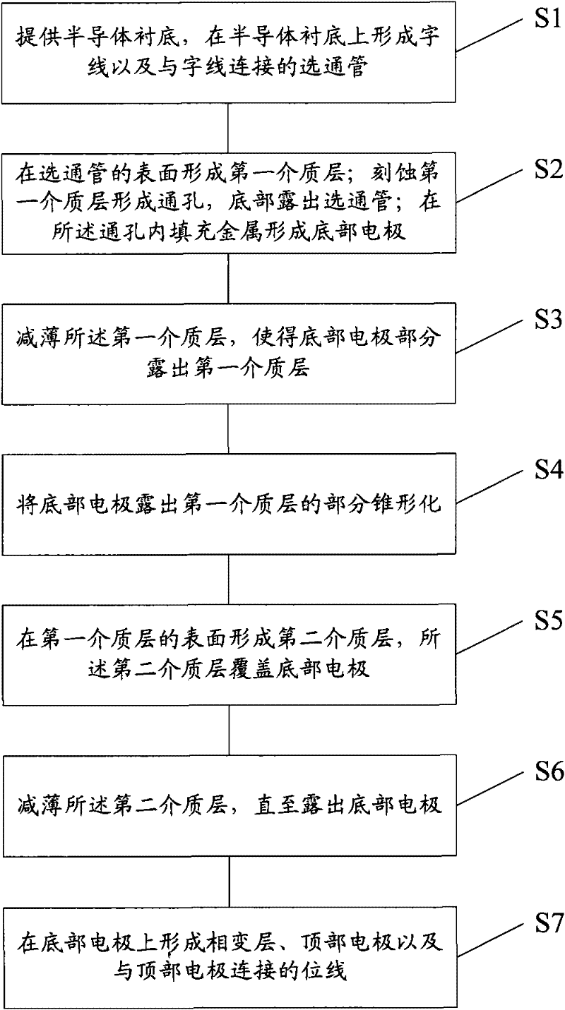
[0039] In the phase change memory formed by the existing manufacturing method, the bottom electrode is in the shape of an inverted trumpet, and the cross section of the top is larger than that of the bottom. Therefore, limited by the existing technology, it is difficult to further reduce the contact area with the phase change layer. The present invention By tapering the top end of the bottom electrode, the cone top forms an ohmic contact with the phase change layer, thereby achieving the purpose of reducing the contact area.

[0040] Such as figure 2 As shown, the phase change memory of the present invention includes:

[0041] Word line 1, bit line 2, phase change memory unit 3, and gate transistor 4;

[0042] The phase-change memory cell 3 includes a bottom electrode 301, a top electrode 303, and a phase-change layer 302 between the bottom electrode 301 and the top electrode 303; one end of the gate transistor 4 is electrically connected to the word line 1, and the other en...


PUM

PropertyMeasurementUnit
thicknessaaaaaaaaaa
thicknessaaaaaaaaaa
diameteraaaaaaaaaa

Abstract

The invention provides a phase change random access memory (RAM) and a manufacturing method thereof. The phase change RAM comprises a word line, a bit line, a phase change RAM unit and a gate tube, wherein the phase change RAM unit comprises bottom electrodes, top electrodes and a phase change layer between the bottom electrodes and the top electrodes; one end of the gate tube is electrically connected with the word line and the other end thereof is electrically connected with the bottom electrodes; the top electrodes are electrically connected with the bit line; the ends at which the bottom electrodes are connected with the phase change layer are shaped like inverted cone; and the vertexes of the cones are in ohmic contact with the phase change contact. Compared with the existing phase change RAMs, the phase change RAM of the invention has the advantage that the bottom electrodes have excellent heating effects on the phase change layer under equivalent driving current, thus improvingthe read-write speed of the phase change RAM.

Description

technical field [0001] The invention relates to a semiconductor memory, in particular to a phase change memory (PCRAM, Phase changeRAM) and a manufacturing method thereof. Background technique [0002] As an emerging non-volatile storage technology, phase change memory has great advantages over flash memory FLASH in many aspects such as read and write speed, read and write times, data retention time, unit area, and multi-value realization. The focus of non-volatile storage technology research. The continuous progress of phase change memory technology makes it one of the most powerful competitors for mainstream products in the future non-volatile memory technology market. [0003] In phase-change memory, the value of the memory can be changed by heat-treating the phase-change layer on which data is recorded. The phase change material constituting the phase change layer enters a crystalline state or an amorphous state due to the heating effect of an applied electric current....

Claims


Application Information

Patent Timeline
Patent Type & Authority Patents(China)
IPC IPC(8): H01L27/24H01L45/00H01L21/82C23F1/02
Inventor 洪中山何其旸
Owner SEMICON MFG INT (SHANGHAI) CORP
Features
  • R&D
  • Intellectual Property
  • Life Sciences
  • Materials
  • Tech Scout
  • Unparalleled Data Quality
  • Higher Quality Content
  • 60% Fewer Hallucinations
Learn More