Semiconductor device, semiconductor device manufacturing method, printed circuit board and electronic device

A manufacturing method and semiconductor technology, applied in semiconductor/solid-state device manufacturing, semiconductor devices, semiconductor/solid-state device components, etc., can solve the problems of large number of decoupling capacitors, large parasitic inductance, large installation area, etc., to achieve Effects of reducing parasitic inductance, reducing switching noise, and reducing voltage fluctuations

Inactive Publication Date: 2011-01-26
NEC CORP +1
View PDF4 Cites 5 Cited by
  • Summary
  • Abstract
  • Description
  • Claims
  • Application Information

AI Technical Summary

Problems solved by technology

However, in general, the number of decoupling capacitors used to suppress such DC voltage fluctuations is large, and the mounting area is large, and there is a problem of increasing the area of ​​the printed circuit board and the resulting increase in cost.
In addition, if the wiring distan

Method used


Image

  • Semiconductor device, semiconductor device manufacturing method, printed circuit board and electronic device
  • Semiconductor device, semiconductor device manufacturing method, printed circuit board and electronic device
  • Semiconductor device, semiconductor device manufacturing method, printed circuit board and electronic device

Examples


Embodiment approach

[0208] Hereinafter, embodiments of the present invention will be described in detail with reference to the drawings.

Embodiment approach 1

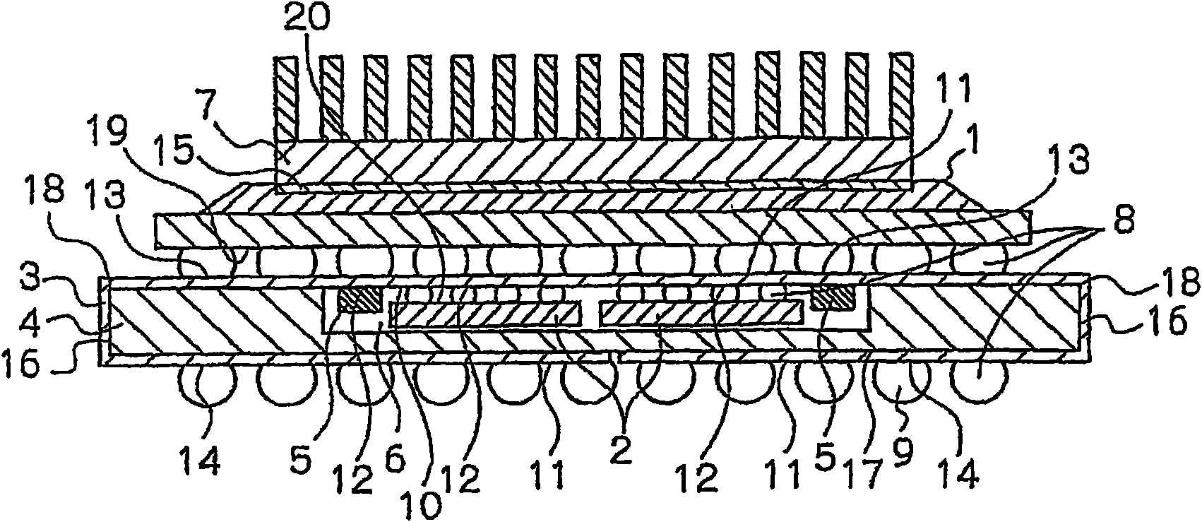
[0210] Figure 1A ~ Figure 1C It is a cross-sectional view showing the semiconductor device according to Embodiment 1 of the present invention. figure 2 It is a plan view (viewed from directly above) when a plurality of memory devices 2 and a plurality of passive components 5 are planarly mounted on the first surface of the flexible circuit board 3 used in the semiconductor device of the present invention. image 3 After a plurality of storage devices 2 and a plurality of passive components 5 are mounted on the flexible circuit board 3, the support body 4 provided with the groove 6 for accommodating these components is bonded to the flexible circuit board 3 in a manner to surround these components. A plan view (viewed from directly above) on the first surface 10 or after being connected to the first external electrode 12 formed on the first surface 10 . Figure 4 is shown along image 3 A diagram of the profile of the line A-A' in.

[0211] Figure 1A The shown semiconduc...

Embodiment approach 2

[0247] Figure 11 It is a cross-sectional view showing a semiconductor device according to Embodiment 2 of the present invention. Figure 11 Embodiment 2 of the present invention shown has a structure similar to Embodiment 1 of the present invention shown in FIG. package) structure) is different from Embodiment 1.

[0248] exist Figure 11 2 shows a structure in which BGA-type packages are stacked in two stages, however, it is not limited to BGA-type packages, and may be a structure in which TSOP-type packages having wiring on external terminals are stacked. also, Figure 11 2 shows a method in which two sets of packages are stacked in two stages, but three or more sets may be used as long as the area limit permits. In addition, as long as the height limit allows, the package can also be stacked more than 3 levels, and it can also include non-stacked packages. Furthermore, even a single package may include a multi-chip package including a plurality of memory dies inside. ...


PUM

PropertyMeasurementUnit
Thicknessaaaaaaaaaa
Linear expansion rateaaaaaaaaaa

Abstract

Provided is a semiconductor device which includes a flexible circuit board whereupon a first external electrode is arranged on a first surface and second and third external electrodes are arranged on a second surface; a plurality of memory devices and passive components; a supporting body having a groove on one surface; and an arithmetic processor device. The memory devices and the passive components are connected to the first external electrode, the one surface of the supporting body is bonded on the first surface of the flexible circuit board so that a groove stores the memory devices and the passive components. The flexible circuit board is bent along the periphery of the supporting body, and wraps the side surfaces and the other surface of the supporting body. On the flexible circuit board, the second external electrode is arranged on the second surface which faces the first external electrode, and the third external electrode is arranged on the second surface which is bent to the other surface of the supporting body. The arithmetic processor device is connected to the second external electrode, and a bump is formed on the third external electrode.

Description

technical field [0001] The present invention relates to a semiconductor device, a method of manufacturing the semiconductor device, and a printed circuit board and electronic equipment on which the semiconductor device is mounted. In particular, it relates to a small semiconductor device that combines an arithmetic processor, a plurality of memory devices, and / or a plurality of passive components, a method for manufacturing the same, and the like. Background technique [0002] Figure 20 A printed circuit board on which semiconductor components are mounted using a related mounting technology (Surface Mount Technology [SMT, Surface Mount Technology]) is shown, which is (one of) related semiconductor devices. This semiconductor device is characterized by a structure in which a plurality of memory packages 102 (for example, DRAM packages) and a plurality of passive components 103 (capacitors, resistors, inductors, etc.) are arranged two-dimensionally around an arithmetic proces...

Claims


Application Information

Patent Timeline
IPC IPC(8): H01L25/065H01L25/07H01L25/18
CPCH01L2924/09701H01L25/105H01L2224/73265H01L2225/06575H01L2224/32225H01L25/0657H01L2924/19105H01L23/4985H01L2225/1094H01L2224/48091H01L2224/16225H01L2924/3511H01L2924/30107H01L2924/01079H01L2225/0651H01L25/16H01L2924/15311H01L2224/73204H01L2224/32145H01L2225/06517H01L21/50H01L2225/1058H01L2224/16145H01L2225/06513H01L2224/45144H01L25/18H01L2924/00H01L2924/00014
Inventor 山崎隆雄渡边真司增田静昭铃木克彦
Owner NEC CORP
Why Eureka
Try Eureka