Impedance matching method and plasma processing equipment
A technology for impedance matching and processing equipment, applied in the field of microelectronics, can solve the problems of poor matching path, low matching accuracy, and long matching time of the actuator, and achieve the effect of efficient application, improved calculation accuracy, and impedance matching.
- Summary
- Abstract
- Description
- Claims
- Application Information
AI Technical Summary
Problems solved by technology
Method used
Image
Examples
Embodiment Construction
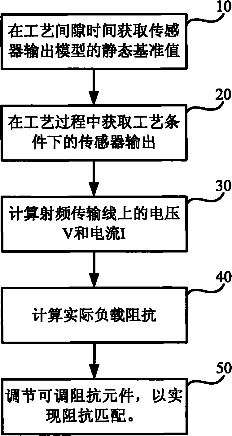
[0040] The technical core of the present invention is: considering the problem that the analog circuit in the sensor will drift over time, the sensor output value is obtained during the process gap time, and it is used as the sensor output in the next process / procedure The static reference value of the model, in order to replace the static reference value of the constant quantity adopted in the background technology with the static reference value that changes with time, thus can obtain the voltage V and the current I on the radio frequency transmission line more accurately, and then more Accurately obtain the load impedance value, and accordingly realize the impedance matching between the internal impedance of the RF power supply and the load impedance.
[0041] In order to enable those skilled in the art to better understand the technical solutions of the present invention, the impedance matching method and plasma processing equipment provided by the present invention will be...
PUM
 Abstract
Description
Claims
Application Information


