Metal-semiconductor field effect transistor with stepped buffer layer structure
A technology of field effect transistors and metal semiconductors, applied in the field of power semiconductor devices, to achieve the effects of improving high-frequency small signal characteristics, reducing parasitic series resistance, and high output power density
- Summary
- Abstract
- Description
- Claims
- Application Information
AI Technical Summary
Problems solved by technology
Method used
Image
Examples
Embodiment Construction
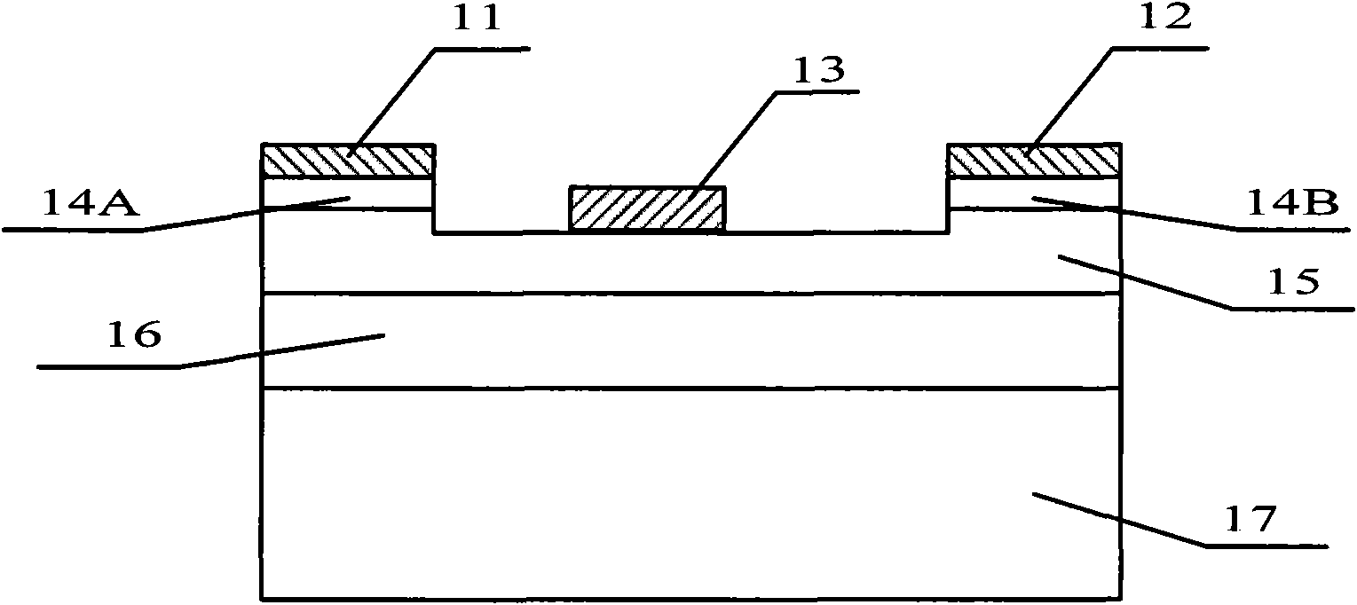
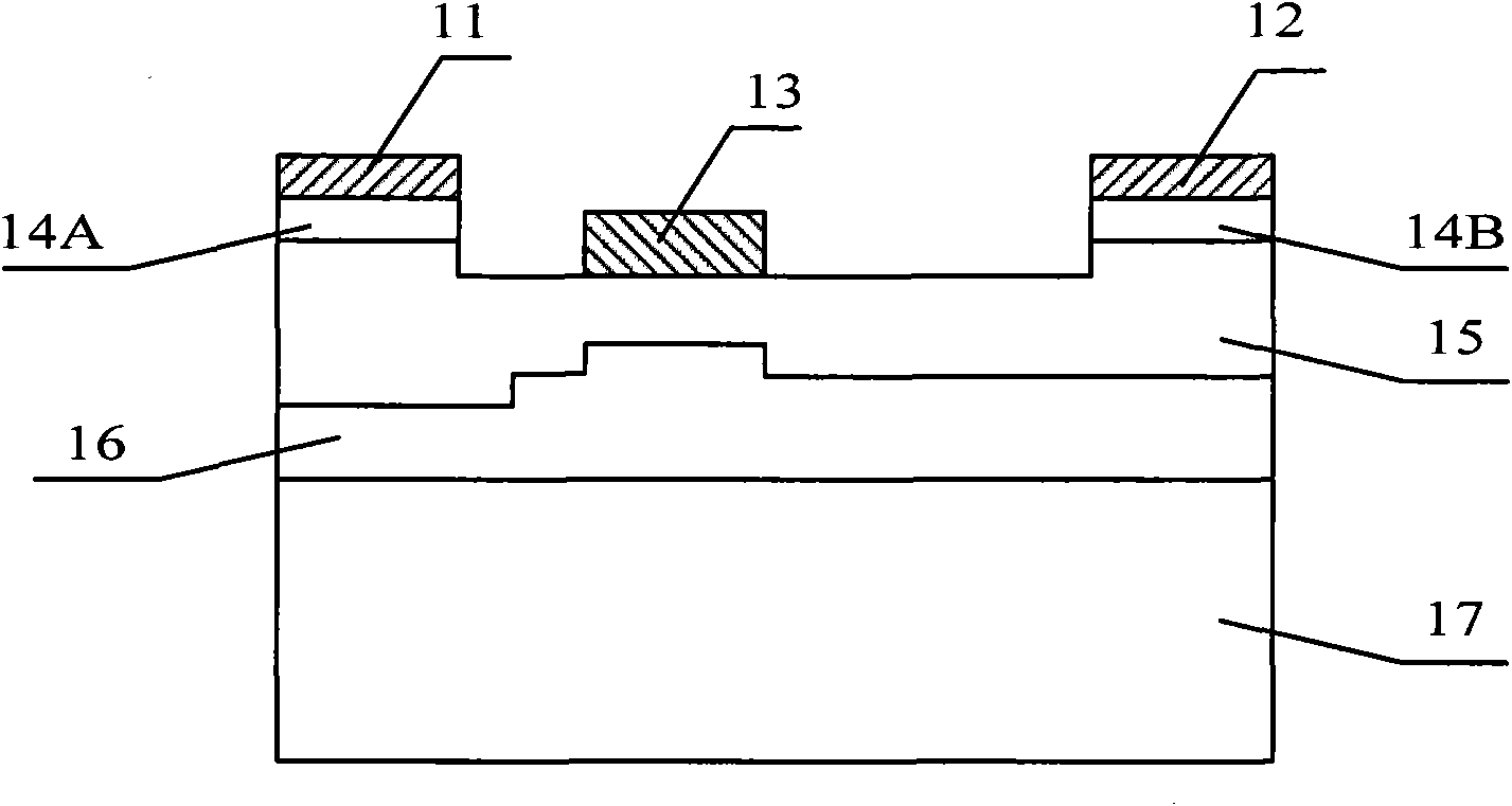
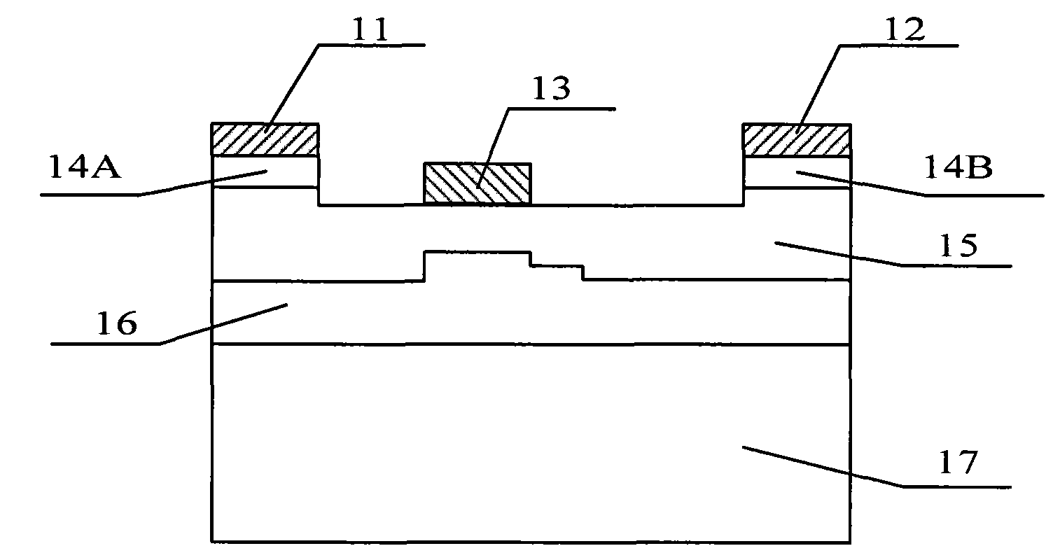
[0021] A metal-semiconductor field-effect transistor with a stepped buffer layer structure, such as Figure 2 to Figure 7 As shown, it includes a semi-insulating substrate 17, a buffer layer 16, an active layer 15, a highly doped ohmic contact region 14A under the source electrode, a highly doped ohmic contact region 14B under the drain electrode, and the source electrode 11 and the drain electrode. 12 and gate electrode 13. The buffer layer 16 is stepped, wherein the part with the largest thickness of the buffer layer 16 appears directly below the gate electrode 13, while the thickness of the buffer layer below the two sides of the gate electrode 13 is relatively small; corresponding to the stepped buffer layer 16 , the active layer 15 is in the shape of an inverted ladder, wherein the thinnest part of the active layer 15 appears directly below the gate electrode 13 , and the thickness of the active layer 15 below both sides of the gate electrode 13 is relatively thick.
[0...
PUM
 Abstract
Description
Claims
Application Information


