Semiconductor photoelectric structure for improving light extraction efficiency and manufacturing method thereof

An extraction efficiency, semiconductor technology, applied in semiconductor devices, circuits, electrical components, etc., to improve light extraction efficiency, reduce defect density, and improve epitaxy quality.

Inactive Publication Date: 2011-02-02
ZHANJING TECH SHENZHEN +1
View PDF2 Cites 40 Cited by
  • Summary
  • Abstract
  • Description
  • Claims
  • Application Information

AI Technical Summary

Problems solved by technology

Although the above method can improve the light extraction efficiency, there are problems o

Method used


Image

  • Semiconductor photoelectric structure for improving light extraction efficiency and manufacturing method thereof
  • Semiconductor photoelectric structure for improving light extraction efficiency and manufacturing method thereof
  • Semiconductor photoelectric structure for improving light extraction efficiency and manufacturing method thereof

Examples


Example Embodiment

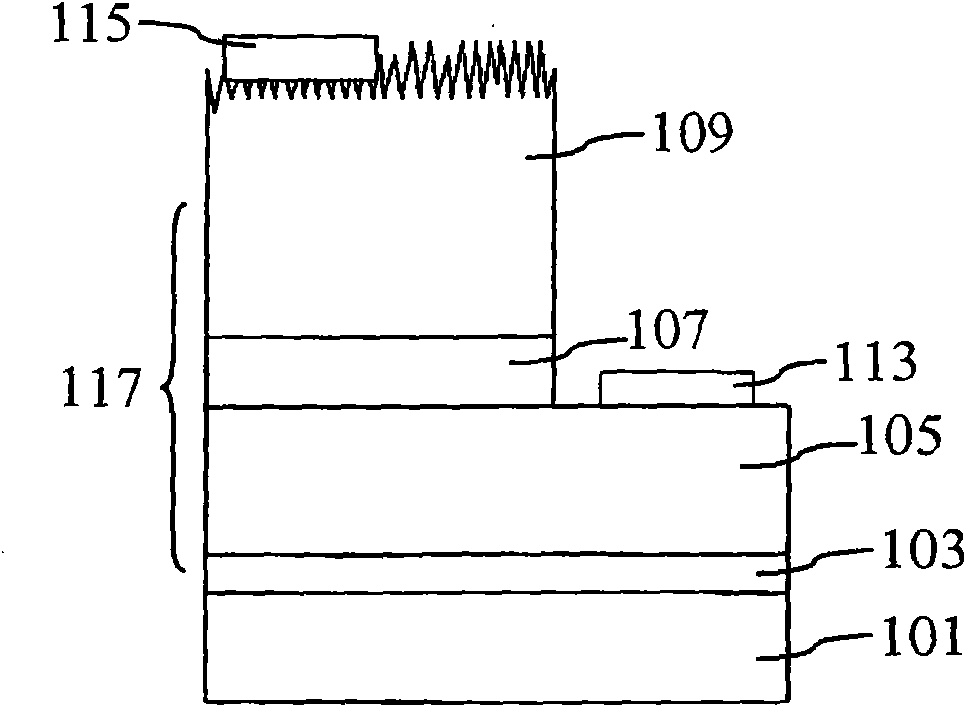
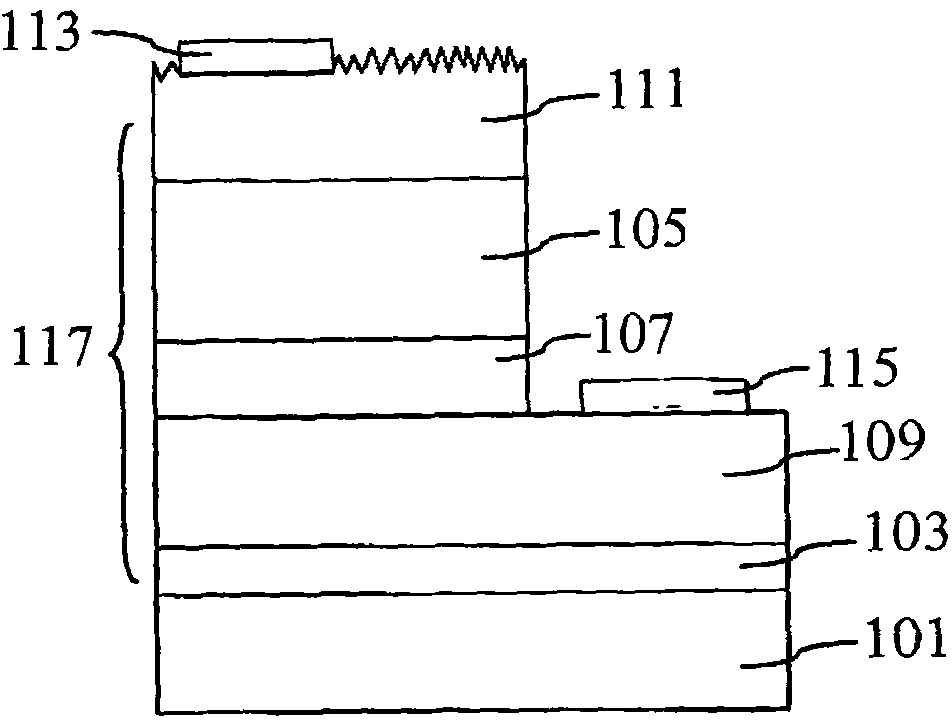
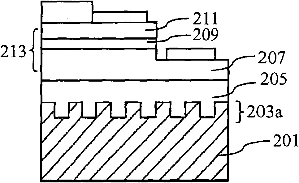
[0073] The direction of the present invention discussed here is a semiconductor optoelectronic device structure and its manufacturing method for improving light extraction efficiency. In order to thoroughly understand the present invention, detailed steps and their composition will be proposed in the following description. Obviously, the implementation of the present invention is not limited to the specific details known to those skilled in semiconductor optoelectronic technology. On the other hand, well-known components or steps are not described in details to avoid unnecessary limitation of the present invention. The preferred embodiments of the present invention will be described in detail as follows. However, in addition to these detailed descriptions, the present invention can also be widely implemented in other embodiments, and the scope of the present invention is not limited, and the following claims shall prevail. .

[0074] An object of the present invention is to imp...


PUM


Abstract

The invention relates to a semiconductor photoelectric structure for improving light extraction efficiency and a manufacturing method thereof. The semiconductor photoelectric structure comprises a substrate and a buffer layer positioned on the substrate, wherein the buffer layer is provided with a continuous hole pattern between the buffer layer and the substrate; a semiconductor layer is positioned on the buffer layer, and comprises an n-type conduction layer positioned on the buffer layer, a light emitting layer positioned on the n-type conduction layer, a p-type conduction layer positionedon the light emitting layer, a transparent electrically-conductive layer positioned on the semiconductor layer, a p-type electrode positioned on the transparent electrically-conductive layer, and an n-type electrode positioned on the n-type conduction layer. Continuous holes are formed below the light emitting layer to reflect the light emitted by the light emitting layer, so that the light intensity and luminance of a light emitting surface are improved. In addition, the defect density of an epitaxy can be reduced, and the quality of the epitaxy can be improved.

Description

technical field [0001] The invention relates to a structure of a group III nitride semiconductor light-emitting element and a manufacturing method thereof, in particular to a structure for improving light extraction rate and a manufacturing method thereof. Background technique [0002] The traditional light-emitting diode structure is limited by total reflection and transverse waveguide effect, so it is impossible to take out all the light generated by the light-emitting layer, and some of it will be absorbed by internal components such as active layer, buffer layer, material defects, and metal electrodes, making the light-emitting diode as a whole The light extraction rate is low. [0003] Taking the blue-white gallium nitride (GaN) group III nitride light-emitting diode as an example, the refractive index of gallium nitride (GaN) is 2.5, and the refractive index of air is 1. Assuming that the light is emitted on a uniform optical surface, it can be calculated The critical...

Claims


Application Information

Patent Timeline
IPC IPC(8): H01L33/00
Inventor 黄世晟涂博闵吴芃逸林文禹马志邦洪梓健沈佳辉
Owner ZHANJING TECH SHENZHEN
Why Eureka
Try Eureka