Low power consumption scanning test circuit and operation method
A scanning test, low power consumption technology, applied in the direction of measuring electricity, measuring electrical variables, measuring devices, etc., to ensure normal operation and reduce dynamic power consumption
- Summary
- Abstract
- Description
- Claims
- Application Information
AI Technical Summary
Problems solved by technology
Method used
Image

Examples
Embodiment Construction
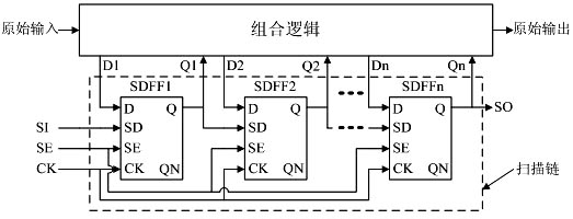
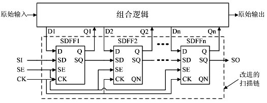
[0029] image 3 The block diagram of the low-power scan test structure is shown. During the process of moving the test vector in and the test result out of the scan chain, the data output from the scan flip-flop to the combinatorial logic remains logic '0', thereby greatly reducing power consumption.
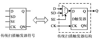
[0030] image 3 Among them, SDFF1, SDFF2, ..., SDFFn are low-power scan flip-flops, SI is the scan input terminal, SE is the scan control terminal ('0' is the normal working mode, '1' is the scan test mode), CK is Scanning clocks, D1, D2, ..., Dn are output signals of the combinational logic, Q1, Q2, ..., Qn are signals output from the scan flip-flops to the combinational logic. Different from the traditional scan structure, the scan input (SD) of each scan flip-flop is connected to the SQ end of the previous scan flip-flop. During the scan shifting process of the test vector from SDFF1 to SDFFn and the process of moving the test result out of the scan chain, the output Q term...
PUM
 Abstract
Description
Claims
Application Information
 - Generate Ideas
- Intellectual Property
- Life Sciences
- Materials
- Tech Scout
- Unparalleled Data Quality
- Higher Quality Content
- 60% Fewer Hallucinations
Browse by: Latest US Patents, China's latest patents, Technical Efficacy Thesaurus, Application Domain, Technology Topic, Popular Technical Reports.
© 2025 PatSnap. All rights reserved.Legal|Privacy policy|Modern Slavery Act Transparency Statement|Sitemap|About US| Contact US: help@patsnap.com