

Data readout circuit and readout method of phase-change storage unit
A technology for phase change storage and data readout, which is applied in the data readout circuit and readout field, and can solve the problems of insignificant voltage difference, long time, and restriction of the speed characteristics of phase change memory, and achieve the effect of overcoming parasitic capacitance
- Summary
- Abstract
- Description
- Claims
- Application Information
AI Technical Summary
Problems solved by technology
Method used
Image

Examples
Embodiment Construction
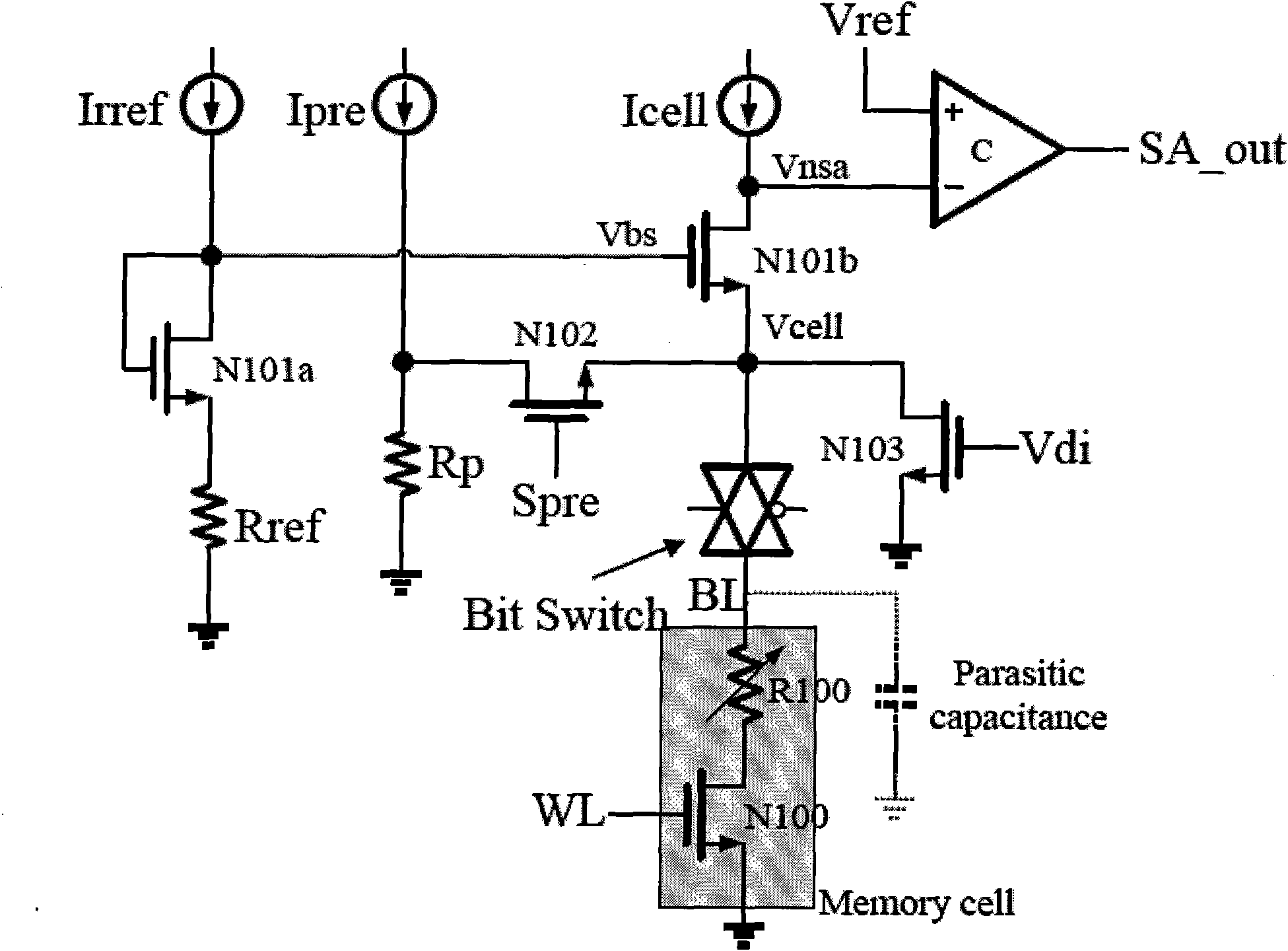
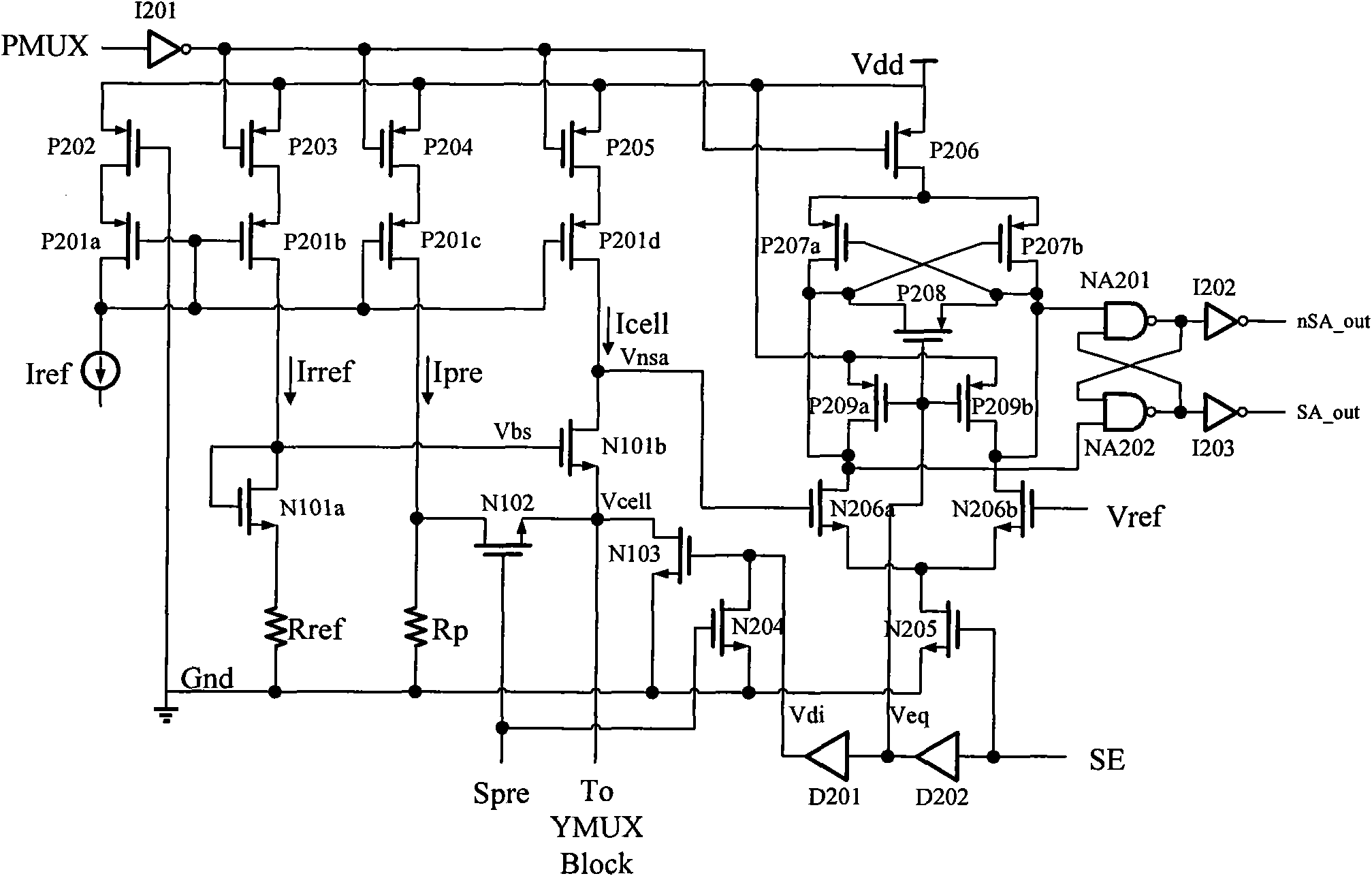
[0020] see figure 1 and figure 2 , The data readout circuit of the phase change memory cell of the present invention at least includes: a read current supply circuit, a decision transistor, a bias voltage generation circuit, a precharge circuit, a comparison circuit, a discharge circuit, and the like. Wherein, the phase-change memory unit to be read (memory cell) adopts a circuit composed of a resistor R100 and a MOS transistor N100 connected in series as an equivalent circuit, and there is a parasitic capacitance (Parasitic Capacitance) on the bit line BL where it is located. In addition, a coupling device Bit Switch, for example, a transmission gate, may be added on the bit line so as to be coupled with other circuits.
[0021] The read current supply circuit is used to provide a read current to the phase-change memory cell to be read during the time period for reading data, and it may use a current source Icell to provide the current. Further, the current source Icell ca...
PUM
 Abstract
Description
Claims
Application Information