

Semiconductor structure and manufacturing method thereof
A manufacturing method and semiconductor technology, applied in the direction of semiconductor devices, semiconductor/solid-state device parts, electric solid-state devices, etc., can solve problems such as hindering chip heat conduction, low heat conduction efficiency, and affecting the reliability of stacked chip packaging structures, etc., to achieve Effect of improving heat dissipation efficiency and improving bonding strength
- Summary
- Abstract
- Description
- Claims
- Application Information
AI Technical Summary
Problems solved by technology
Method used
Image

Examples
Embodiment Construction
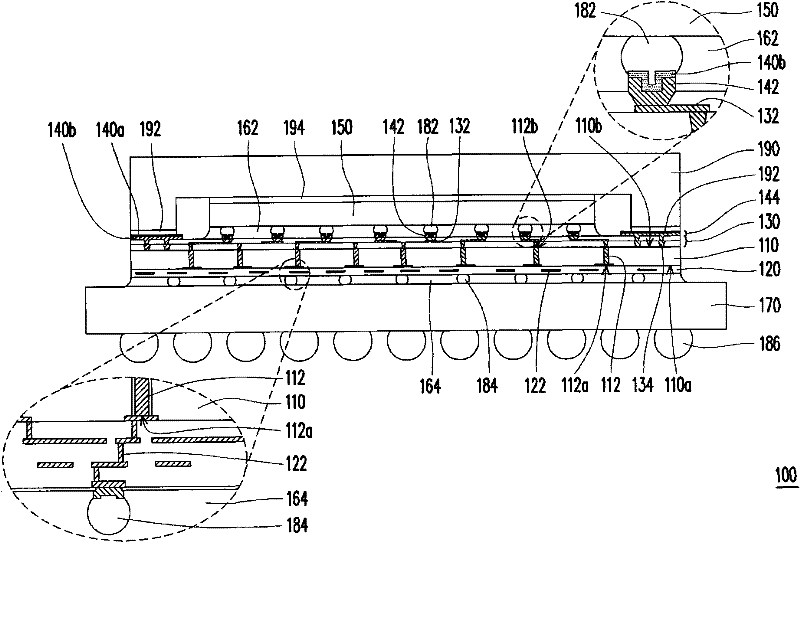
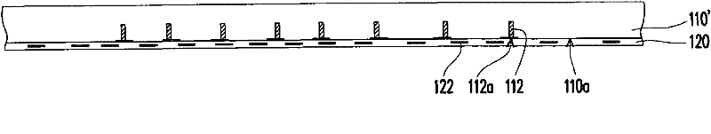
[0058] figure 1 A semiconductor structure according to an embodiment of the invention is shown. Such as figure 1As shown, the semiconductor structure 100 includes a first chip 110 , wherein the first chip 110 has a plurality of TSVs 112 inside. A first wiring layer 120 is disposed on the active surface 110 a of the first chip 110 . Here, the first wiring layer 120 includes a first interconnection 122 , which is, for example, an interconnection formed in a back end of line (BEOL) process in the wafer fabrication process. The first interconnection 122 is, for example, connected between one end 112 a of the TSV 112 and the second conductive bump 184 under the first chip 110 . In addition, there may be other active or passive components (not shown) in the first chip 110 , so the first interconnection 122 may also be connected to these active or passive components.
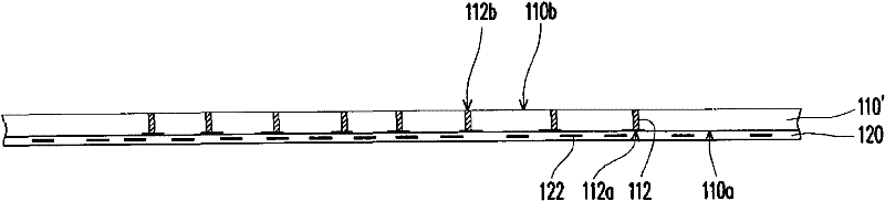
[0059] The second wiring layer 130 is disposed on the back surface 110 b of the first chip 110 . The second wir...
PUM
 Abstract
Description
Claims
Application Information