Touch panel and repair method thereof

A touch panel and repair wire technology, applied in the direction of instrument, electrical digital data processing, data processing input/output process, etc., can solve the problem that X sensing serial or Y sensing serial cannot operate normally, metal bridge wire Problems such as short circuit or open circuit

Active Publication Date: 2011-03-09
AU OPTRONICS CORP
View PDF3 Cites 24 Cited by
  • Summary
  • Abstract
  • Description
  • Claims
  • Application Information

AI Technical Summary

Problems solved by technology

However, when the electrostatic discharge phenomenon occurs, the metal bridge wires at the intersection of the X sensing series and the Y sensing series may be blown and short-circuited or disconnected, resulting in the failure of the X sensing series or the Y sensing series. normal operation

Method used


Image

  • Touch panel and repair method thereof
  • Touch panel and repair method thereof
  • Touch panel and repair method thereof

Examples


no. 1 example

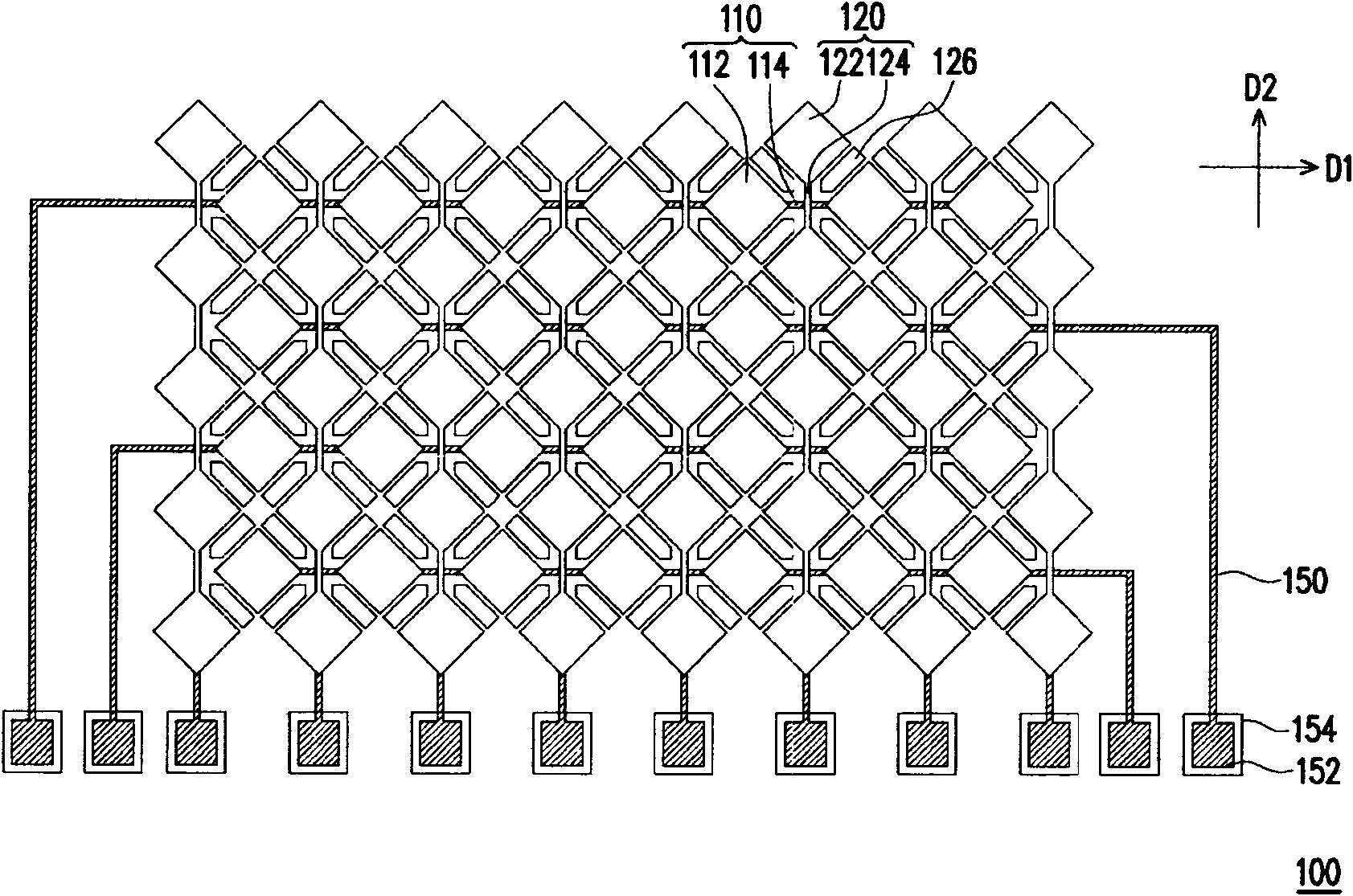
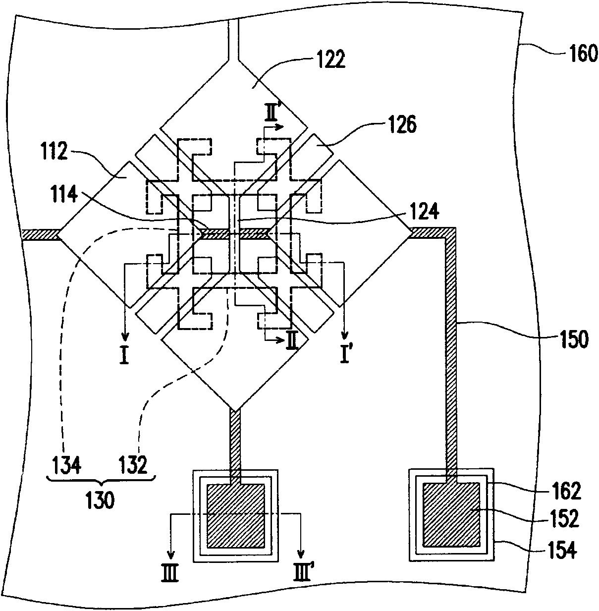
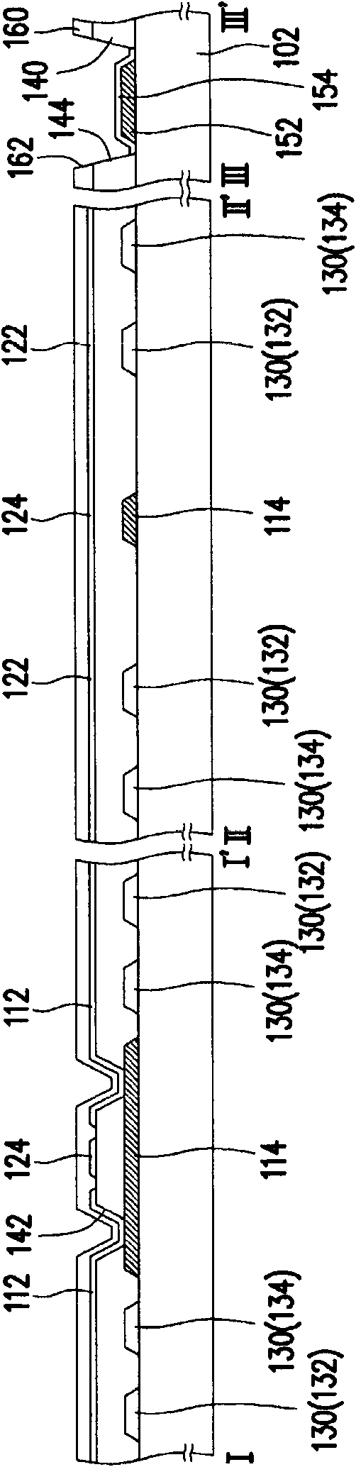
[0063] Figure 1A is a schematic top view of a touch panel according to a first embodiment of the present invention, Figure 1B for Figure 1A A partially enlarged schematic diagram of , and Figure 1C for along Figure 1B Schematic cross-sectional views of line I-I', line II-II' and line III-III'. Please also refer to Figure 1A to Figure 1C , in this embodiment, the touch panel 100 includes a substrate 102, a plurality of first sensing series 110, a plurality of second sensing series 120, a plurality of conductive repair pattern layers 130 and a first dielectric layer 140 . The substrate 102 is, for example, a glass substrate, a plastic substrate, a flexible substrate or other substrates. The substrate 102 can also be a printed circuit board or a display panel, such as a liquid crystal display panel, an organic display panel, an electrophoretic display panel, a plasma display panel, etc. It can be directly integrated on the display panel or in the display panel. Taking ...

no. 2 example

[0083] Figure 6A It is a schematic top view of a touch panel according to a second embodiment of the present invention, Figure 6B for Figure 6A The partially enlarged schematic diagram of , and Figure 6C for along Figure 6B Schematic cross-sectional views of line I-I', line II-II' and line III-III'. Please also refer to Figure 6A to Figure 6C , in this embodiment, the touch panel 100 includes a substrate 102, a plurality of first sensing series 110, a plurality of second sensing series 120, a plurality of conductive repair pattern layers 130, a first dielectric layer 140 , the second dielectric layer 160 and a plurality of peripheral connection lines 150 and a plurality of peripheral connection pads 152 . In this embodiment, the first dielectric layer 140 is, for example, disposed on the substrate 102 and has a plurality of vias 142 .

[0084] In this embodiment, the first sensing series 110 is disposed on the substrate 102 and extends along a first direction D1, w...


PUM


Abstract

The invention discloses a touch panel and a repair method thereof. The touch panel comprises a substrate, a plurality of first sensing universal serial buses, a plurality of second sensing universal serial buses and a plurality of conductive repair pattern layers, wherein the first sensing universal serial buses are configured on the substrate, extend in the first direction, and comprise a plurality of first sensing pads and a plurality of first bridging lines; each first bridging line is used for connecting every two adjacent first sensing pads in series; the second sensing universal serial buses are configured on the substrate, extend in the second direction, and comprise a plurality of second sensing pads and a plurality of second bridging lines; each second bridging line is used for connecting every two adjacent second sensing pads in series; the first direction is different from the second direction; the first sensing universal serial buses are electrically insulated from the second sensing universal serial buses; the conductive repair pattern layers are positioned close to the junctures of the first and second universal serial buses; and the conductive repair pattern layers are electrically floated, and can connect every two adjacent sensing pads after the repair movement finishes.

Description

【Technical field】 [0001] The present invention relates to a panel and its repairing method, and in particular to a touch panel and its repairing method. 【Background technique】 [0002] According to different sensing methods, touch panels are roughly classified into resistive touch panels, capacitive touch panels, optical touch panels, acoustic wave touch panels, and electromagnetic touch panels. Since the capacitive touch panel has the advantages of fast response time, good reliability and high durability, the capacitive touch panel has been widely used in electronic products. According to different structures and manufacturing methods, capacitive touch panels can be roughly divided into two types: surface-mounted and integrated / in-cell. In the surface-mounted capacitive touch panel, the sensing series is usually fabricated on a substrate, and then the substrate with the sensing series is attached to the outer surface of the display. Obviously, the outer The stick-type tou...

Claims


Application Information

Patent Timeline
Patent Type & Authority Applications(China)
IPC IPC(8): G06F3/041
Inventor 詹立雄曾贤楷廖金阅周鸿文
Owner AU OPTRONICS CORP
Why Eureka
Try Eureka