All-in-one machine of semiconductor device for testing, sorting, marking and braiding and one-stop processing method

A processing method and semiconductor technology, applied in the direction of semiconductor/solid-state device testing/measurement, semiconductor/solid-state device manufacturing, electrical components, etc., can solve problems such as waste of labor, complicated operation, and failure to meet market demand, so as to improve work efficiency, The effect of guaranteeing the pass rate

Active Publication Date: 2011-03-23
深圳市复德科技有限公司
4 Cites 35 Cited by

AI-Extracted Technical Summary

Problems solved by technology

[0003] In the existing technology, most of the semiconductor device processing automation equipment in my country are single-program processing equipment, such as: semiconductor chip testing machine, semiconductor chip tape machine, semiconductor chip sorting machine, semiconductor chip marking machin...

Method used

Enter next station namely visual imaging direction detection system 5, by photosensitive system photosensitive, whether the direction of detection semiconductor device is correct, as incorrect, enter next station namely high-speed correction positioning and steering system 6 and carry out correction positioning and Turning to next, the real-time detection system of the electrical performance parameters of the semiconductor device is carried out. According to the prior settings, different parameters are respectively detected at the real-time detection system A of the electrical performance parameters and the real-time detection system B of the...

Abstract

The invention discloses an all-in-one machine of a semiconductor device for testing, sorting, marking and braiding and a one-stop processing method. A scheme in the invention is as follows: the semiconductor device is transported to a device processing system arranged on each station to be processed by the all-in-one machine. The all-in-one machine comprises a machine body and each device processing system, wherein the machine body is provided with a main turret system and a laser marking turret system respectively with 16 working positions; each station of the main turret system is provided with a suction nozzle mechanism for picking, placing and transporting the device; the main turret system is also provided with a suction nozzle pressing mechanism; each station of the laser marking turret system is provided with a device transmission mechanism; and the suction nozzle mechanism and the device transmission mechanism successively transmit the semiconductor device to each device processing system to finish one-stop continuous processing. By the implementation of the invention, various functions such as testing, sorting, marking, braiding, outputting and the like which originally need to be finished by various equipment are finished on one equipment, thus saving cost and improving working efficiency.

Application Domain

Semiconductor/solid-state device testing/measurementSemiconductor/solid-state device manufacturing +2

Technology Topic

Embedded systemSemiconductor +5

Image

  • All-in-one machine of semiconductor device for testing, sorting, marking and braiding and one-stop processing method
  • All-in-one machine of semiconductor device for testing, sorting, marking and braiding and one-stop processing method
  • All-in-one machine of semiconductor device for testing, sorting, marking and braiding and one-stop processing method

Examples

  • Experimental program(1)
  • Effect test(1)

Example Embodiment

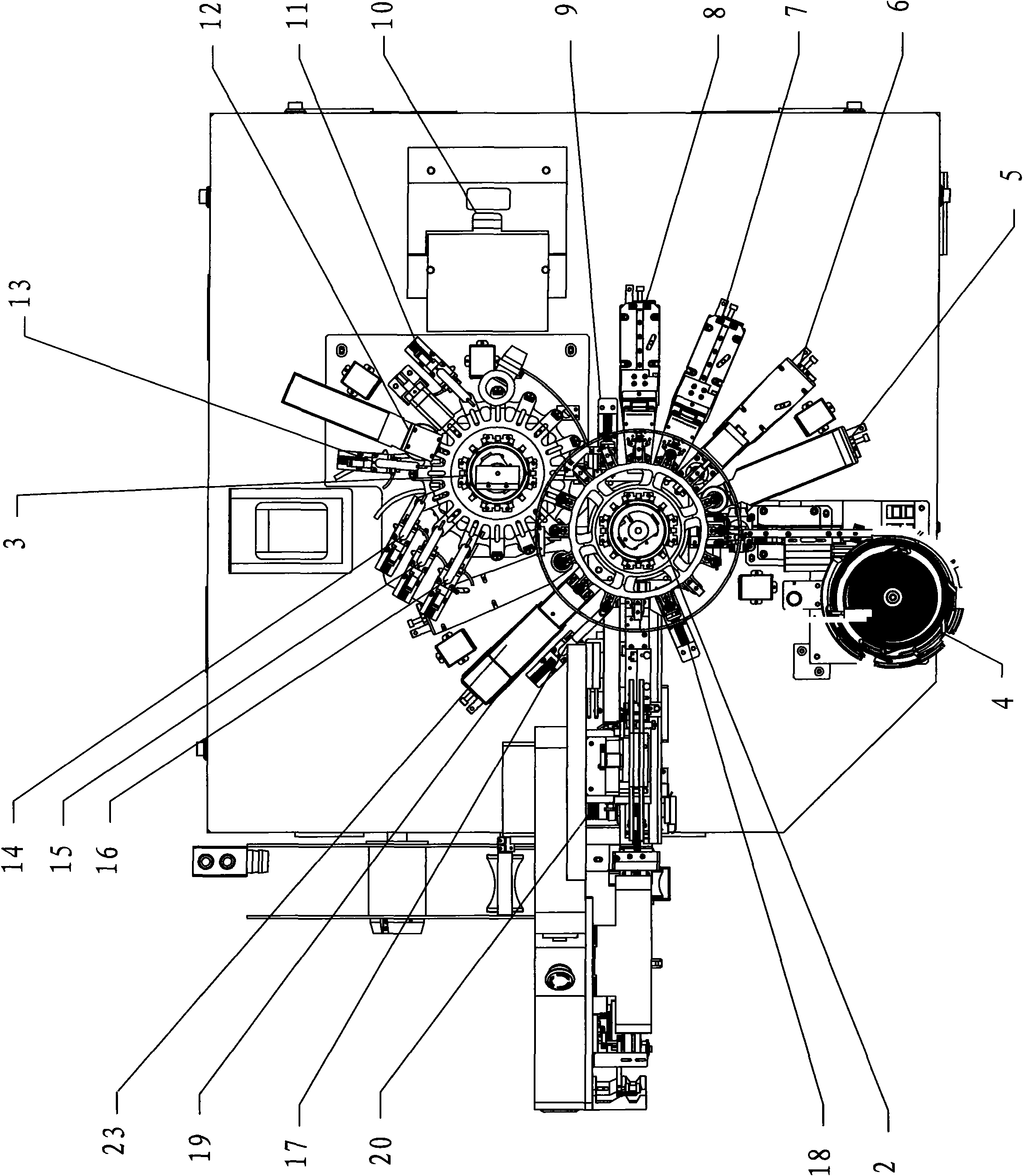
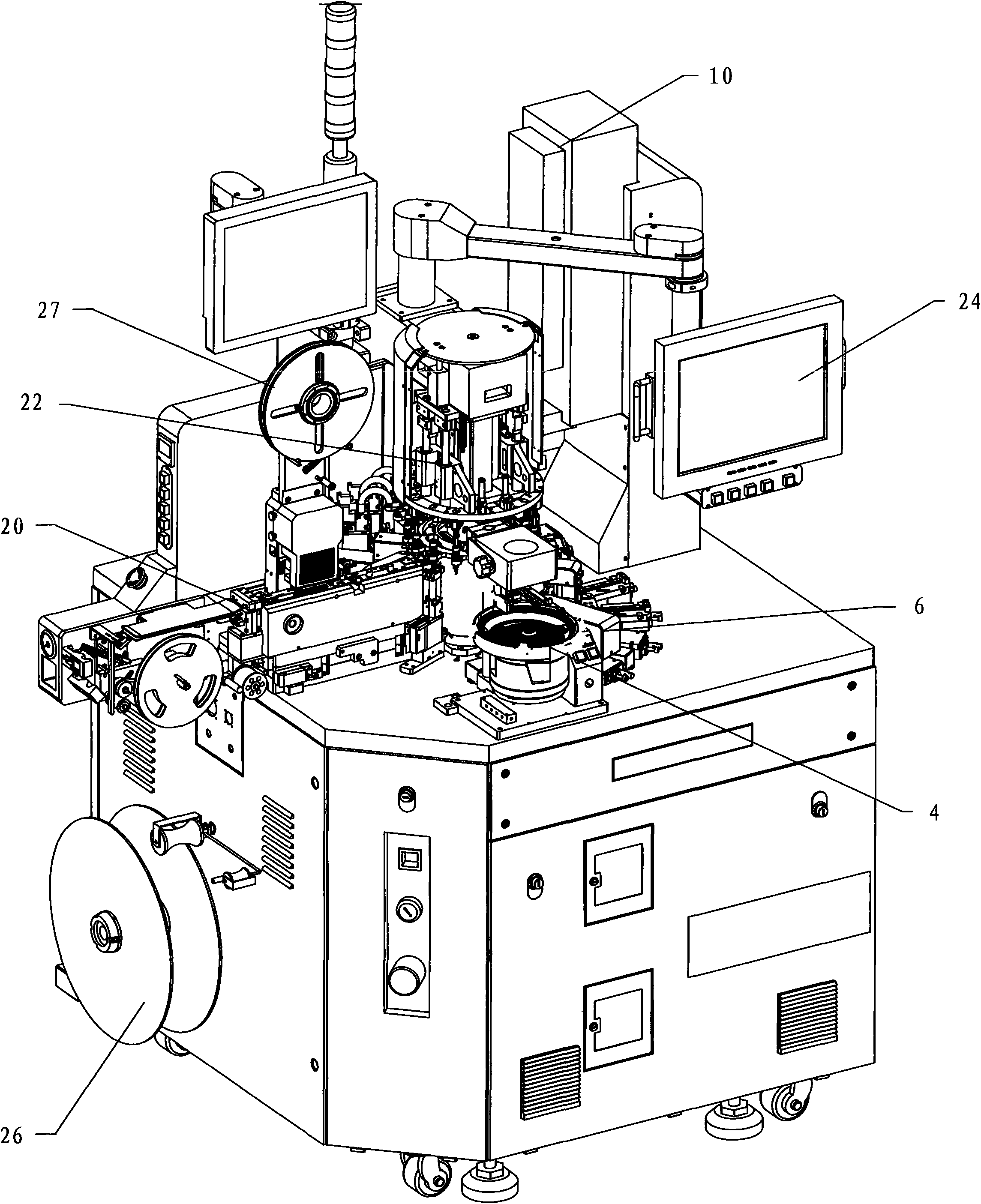
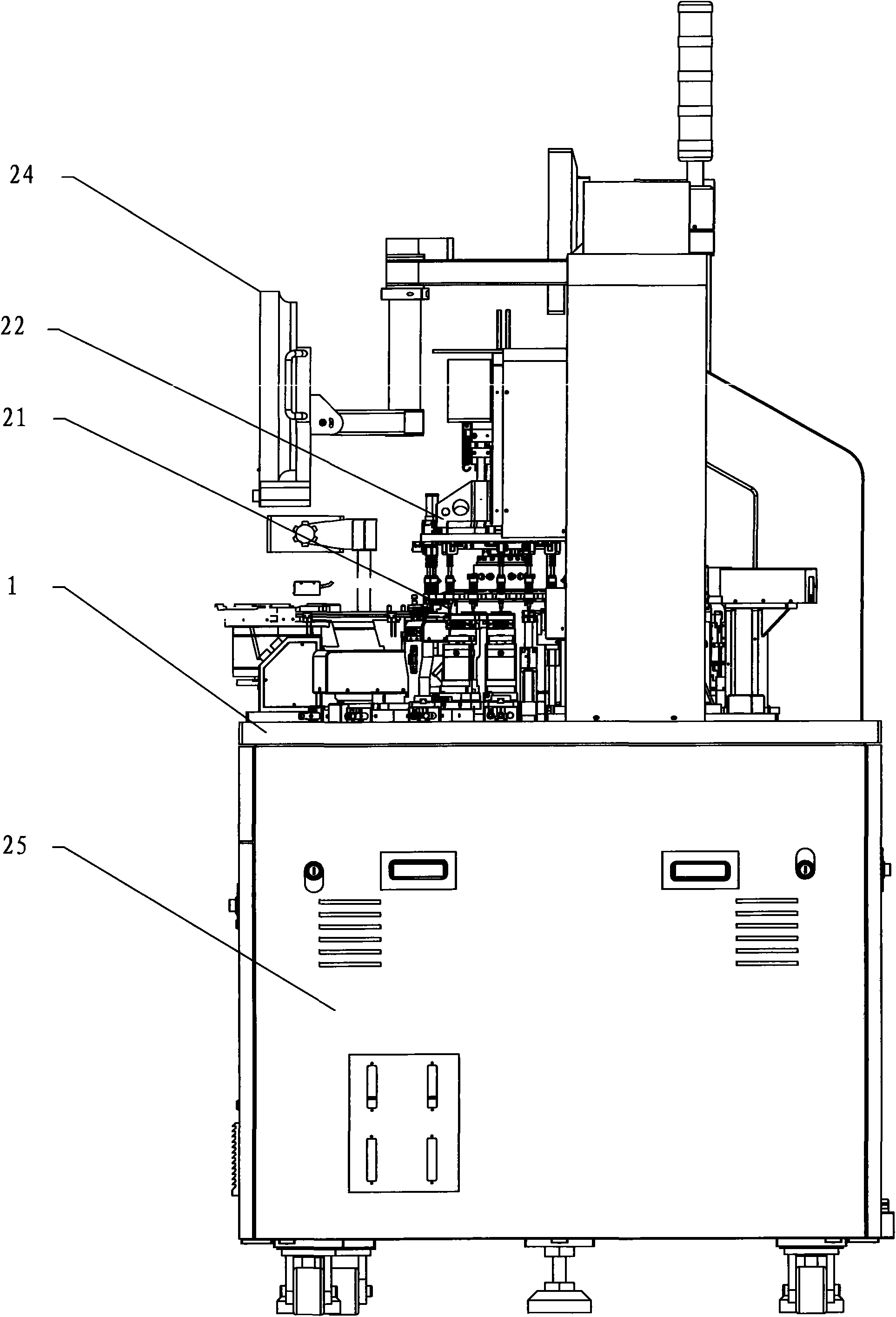
[0038] Such as figure 1 , figure 2 , image 3 , Figure 4 As shown, figure 1 It is the working position and station distribution diagram of the main turret system and the laser marking turret system of the present invention, figure 2 Is a schematic diagram of the three-dimensional structure of the present invention, image 3 Is a schematic side view of the structure of the present invention, Figure 4 It is a schematic diagram of the station distribution of the device processing system of the present invention. Now combined figure 1 , figure 2 , image 3 , Figure 4 The embodiment of the present invention is described in detail: an integrated machine for testing, sorting, marking and taping of semiconductor devices, including a machine body 1 and various device processing systems that are fixedly connected to the machine body, and a 16 working machine is provided on the machine body 1. The main turret system 2 and a 16-station laser marking turret system 3 matched with it, the corresponding stations on the main turret system 2 and the laser marking turret system 3 Corresponding device processing systems are provided. Each work position of the main turret system 2 is provided with a suction nozzle mechanism 21 for device pick-up and delivery, and the main turret system 2 is also provided The suction nozzle pressing mechanism 22 corresponding to the suction nozzle mechanism 21 for picking, placing and conveying the device is provided with a device conveying mechanism 23 on each working position of the laser marking turret system 3.
[0039] The device processing system includes vibration self-alignment feeding system 4, visual imaging direction detection system 5, high-speed correction positioning and steering system 6, electrical performance parameter real-time detection system A7, electrical performance parameter real-time detection system B8, and laser marking system 10. Visual imaging identification detection system 12, classification selection collection system A9, classification selection collection system B11, classification selection collection system C13, classification selection collection system D14, classification selection collection system E15, classification selection collection system F16, classification selection collection system G17 , Classification, selection and collection system H18, visual imaging 3D size detection system 19 and/or tape and packaging output system 20, and also includes a control system 25, and a display and operating system 24. The control system 25 is set in the machine body 1 Below, the display and operating system 24 is arranged above the machine body 1.
[0040] Place the semiconductor devices in the vibrating disk in the vibrating self-arrangement feeding system 4 in advance, and use the vibrating motor to directionally vibrate. The semiconductor devices can be arranged in an orderly manner, and the wrong directions of the semiconductor devices can be identified and filtered. The vibrating plate port adjusts the semiconductor device to the correct direction, making the feeding more convenient, effective and timely; the supply speed can guarantee the maximum amount of 30,000 pieces/hour, and then it is filtered, and finally transported through the straight discharge track and passed the identification The direction of the semiconductor device, the semiconductor device is sent to the separator.

PUM

no PUM

Description & Claims & Application Information

We can also present the details of the Description, Claims and Application information to help users get a comprehensive understanding of the technical details of the patent, such as background art, summary of invention, brief description of drawings, description of embodiments, and other original content. On the other hand, users can also determine the specific scope of protection of the technology through the list of claims; as well as understand the changes in the life cycle of the technology with the presentation of the patent timeline. Login to view more.

Similar technology patents

Automatic device for welding and detecting lithium battery

ActiveCN103904367AShorten the running distanceImprove work efficiency
Owner:DONGGUAN HONBRO LI BATTERY EQUIP TECH

Vacuum cleaner

InactiveCN103356140Aprevent liftingImprove work efficiency
Owner:SUZHOU HAAN TECH +1

Classification and recommendation of technical efficacy words

  • Improve work efficiency
  • Guaranteed pass rate

Cooperation service platform facing different source data

InactiveCN101174957AImprove management level and qualityImprove work efficiency
Owner:NANJING UNIV OF FINANCE & ECONOMICS

Screw drilling tool, vertical drilling tool testing method and well inclination simulation testing equipment

InactiveCN111594144AReduced height requirementsImprove work efficiency
Owner:DEZHOU UNITED GASOLINEEUM MACHINERY

Method for intelligent automatic identification of transmission circuit parts

Owner:INFORMATION COMM COMPANY STATE GRID SHANDONG ELECTRIC POWER +2

Keyboard spill-proofing mechanism

ActiveUS7030330B2minimize manufacturing costimprove work efficiency
Owner:LITE ON SINGAPORE PTE LTD

Second metallizing method for ceramics

InactiveCN101224997AGuaranteed pass ratecost control
Owner:CHANGSHU CITY YINYANG CERAMIC CO LTD

Method for detecting etching fluid filter

InactiveCN101769848AReduce the production of defective productsGuaranteed pass rate
Owner:SEMICON MFG INT (SHANGHAI) CORP

Wet type isostatic cool pressing die

InactiveCN106113228AIncrease productivityGuaranteed pass rate
Owner:HUBEI XITIAN TECH CO LTD

Production frame used for processing clutch release bearing of automobile

ActiveCN104259824AGuaranteed pass ratereduce speed
Owner:ZHEJIANG BORRY AUTO PARTS
Why Eureka
Try Eureka